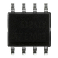
TS512AIYDT STMicroelectronics, TS512AIYDT Datasheet

TS512AIYDT
Specifications of TS512AIYDT
Available stocks
Related parts for TS512AIYDT
TS512AIYDT Summary of contents
Page 1
Features ■ Low input offset voltage: 500 µV max. (A version) ■ Low power consumption ■ Short-circuit protection ■ Low distortion, low noise ■ High gain-bandwidth product: 3 MHz ■ High channel separation ■ ESD protection 2 kV ■ Macromodel ...
Page 2
Absolute maximum ratings and operating conditions 1 Absolute maximum ratings and operating conditions Table 1. Absolute maximum ratings Symbol V Supply voltage CC V Input voltage in V Differential input voltage id Thermal resistance junction to ambient R DIP8 thja ...
Page 3
TS512, TS512A 2 Schematic diagram Figure 1. Schematic diagram (1/2 TS512) R16 4kΩ Q25 Q5 Q6 R15 150kΩ 2kΩ 2kΩ 4kΩ 4kΩ Q13 Q11 Q2 Q12 Q3 Inverting Input Q15 Q7 Q17 Q31 Q32 Q4 Q18 ...
Page 4
Electrical characteristics 3 Electrical characteristics Table Symbol Supply current (per operator ≤ min Input bias current I ≤ min R Input resistance kHz in Input offset voltage ...
Page 5
TS512, TS512A Table Symbol SVR Supply voltage rejection ratio V /V Channel separation kHz ± 25°C (unless otherwise specified) (continued) amb Parameter Doc ID 4948 Rev 4 Electrical ...
Page 6
Electrical characteristics Figure 2. V distribution 25° distribution ° -400 -200 0 Input offset voltage (µV) Figure 4. Input offset voltage vs. ...
Page 7
TS512, TS512A Figure 8. Supply current (per operator) vs. input common mode voltage 0.50 0.50 0.45 0.40 0.40 0.35 0.30 0.30 Follower configuration 0. ...
Page 8
Electrical characteristics Figure 14. Voltage gain and phase for different capacitive loads and T = 25°C icm 50 Gain Phase =600pF =330pF ...
Page 9
TS512, TS512A Figure 20. Phase margin vs. output current icm 70 Recommended area =100 =330 -10 ...
Page 10
Macromodels 4 Macromodels 4.1 Important notes concerning this macromodel ● All models are a trade-off between accuracy and complexity (i.e. simulation time). ● Macromodels are not a substitute to breadboarding; rather, they confirm the validity of a design approach and ...
Page 11
TS512, TS512A FIBN 5 1 VOFP 1.000000E-02 * AMPLIFYING STAGE FIP 5 19 VOFP 9.000000E+02 FIN 5 19 VOFN 9.000000E+02 RG1 19 5 1.727221E+06 RG2 19 4 1.727221E+ 6.000000E-09 DOPM 19 22 MDTH 400E-12 DONM 21 19 ...
Page 12
Package information 5 Package information In order to meet environmental requirements, ST offers these devices in different grades of ® ECOPACK packages, depending on their level of environmental compliance. ECOPACK specifications, grade definitions and product status are available at: www.st.com. ...
Page 13
TS512, TS512A Figure 22. DIP8 package mechanical drawing Table 5. DIP8 package mechanical data Ref Dimensions Millimeters Min. Typ. Max. 5.33 0.38 2.92 3.30 4.95 0.36 0.46 ...
Page 14
Package information Figure 23. SO-8 package mechanical drawing Table 6. SO-8 package mechanical data Ref ccc 14/17 Dimensions Millimeters Min. Typ. Max. 1.75 0.10 0.25 1.25 0.28 ...
Page 15
... TS512IN TS512AIN TS512ID TS512IDT TS512AID TS512AIDT (1) TS512IYD (1) TS512IYDT (1) TS512AIYDT 1. Qualification and characterization according to AEC Q100 and Q003 or equivalent, advanced screening according to AEC Q001 & Q 002 or equivalent are on-going. Temperature Package range DIP8 SO-8 -40°C, + 125°C SO-8 (Automotive grade) Doc ID 4948 Rev 4 ...
Page 16
Revision history 7 Revision history Table 8. Document revision history Date 21-Nov-2001 23-Jun-2005 05-May-2008 04-Feb-2010 16/17 Revision 1 Initial release. PPAP references inserted in the datasheet, see 2 codes. AC and DC performance characteristics curves added for ...
Page 17
... TS512, TS512A Information in this document is provided solely in connection with ST products. STMicroelectronics NV and its subsidiaries (“ST”) reserve the right to make changes, corrections, modifications or improvements, to this document, and the products and services described herein at any time, without notice. All ST products are sold pursuant to ST’s terms and conditions of sale. ...


