TS272CD STMicroelectronics, TS272CD Datasheet
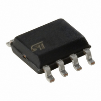
IC OPAMP CMOS DUAL HP 8-SOIC

TS272CD

Manufacturer Part Number
TS272CD
Description
IC OPAMP CMOS DUAL HP 8-SOIC
Manufacturer
STMicroelectronics
Datasheet

Specifications of TS272CD

Amplifier Type
General Purpose
Number Of Circuits
2
Slew Rate
5.5 V/µs
Gain Bandwidth Product
3.5MHz
Current - Input Bias
1pA
Voltage - Input Offset
1100µV
Current - Supply
1mA
Current - Output / Channel
45mA
Voltage - Supply, Single/dual (±)
3 V ~ 16 V, ±1.5 V ~ 8 V
Operating Temperature
0°C ~ 70°C
Mounting Type
Surface Mount
Package / Case
8-SOIC (3.9mm Width)
Number Of Channels
2
Common Mode Rejection Ratio (min)
65 dB
Input Offset Voltage
10 mV
Input Bias Current (max)
150 pA
Operating Supply Voltage
5 V, 9 V, 12 V, 15 V
Supply Current
3 mA
Maximum Operating Temperature
+ 70 C
Minimum Operating Temperature
0 C
Dual Supply Voltage
+/- 3 V, +/- 5 V
Maximum Dual Supply Voltage
+/- 8 V
Minimum Dual Supply Voltage
+/- 1.5 V
Mounting Style
SMD/SMT
Shutdown
No
Supply Voltage (max)
16 V
Supply Voltage (min)
3 V
Technology
CMOS
Voltage Gain Db
83.52 dB
Lead Free Status / RoHS Status
Contains lead / RoHS non-compliant
Output Type
-
-3db Bandwidth
-
Lead Free Status / Rohs Status
Lead free / RoHS Compliant
Other names
497-3037-5

Available stocks

Company
Part Number
Manufacturer
Quantity
Price
Part Number:
TS272CD
Manufacturer:
STMicroelectronics
Quantity:
1 890
Part Number:
TS272CDP
Manufacturer:
ST
0
Part Number:
TS272CDT
Manufacturer:
ALTERA
0
Part Number:
TS272CDT
Manufacturer:
ST
0
Part Number:
TS272CDT
Manufacturer:
ST
Quantity:
20 000
Company:
Part Number:
TS272CDT
Quantity:
5 000
Part Number:
TS272CDT$D4F
Manufacturer:
ST
0
DESCRIPTION
The TS272 devices are low cost, dual operational
amplifiers designed to operate with single or dual
supplies. These operational amplifiers use the ST
silicon gate CMOS process allowing an excellent
consumption-speed ratio. These series are ideally
suited for low consumption applications.
Three power consumptions are available allowing
to have always the best consumption-speed ratio:
These CMOS amplifiers offer very high input im-
pedance and extremely low input currents. The
major advantage versus JFET devices is the very
low input currents drift with temperature (see fig-
ure 2).
ORDER CODE
N = Dual in Line Package (DIP)
D = Small Outline Package (SO) - also available in Tape & Reel (DT)
P = Thin Shrink Small Outline Package (TSSOP) - only available
November 2001
TS272C/AC/BC
TS272I/AI/BI
TS272M/AM/BM
Example : TS272ACN
Part Number
in Tape & Reel (PT)
OUTPUT VOLTAGE CAN SWING TO
GROUND
EXCELLENT PHASE MARGIN ON
CAPACITIVE LOADS
GAIN BANDWIDTH PRODUCT: 3.5MHz
STABLE AND LOW OFFSET VOLTAGE
THREE INPUT OFFSET VOLTAGE
SELECTIONS
I
I
I
CC
CC
CC
= 10µA/amp.: TS27L2 (very low power)
= 150µA/amp.: TS27M2 (low power)
= 1mA/amp.: TS272 (standard)
Temperature Range
-40°C, +125°C
-55°C, +125°C
0°C, +70°C
CMOS DUAL OPERATIONAL AMPLIFIERS
N
Package
D
P
PIN CONNECTIONS (top view)
(Thin Shrink Small Outline Package)
HIGH PERFORMANCE
1
2
3
4
(Plastic Micropackage)
1 - Output 1
2 - Inverting Input 1
3 - Non-inverting Input 1
4 - V
5 - Non-inverting Input 2
6 - Inverting Input 2
7 - Output 2
8 - V
+
-
(Plastic Package)
CC
CC
TSSOP8
+
-
SO8
DIP8
D
N
P
TS272C,I,M
+
-
8
7
6
5
1/9

Related parts for TS272CD

TS272CD Summary of contents

Page 1

OUTPUT VOLTAGE CAN SWING TO GROUND EXCELLENT PHASE MARGIN ON CAPACITIVE LOADS GAIN BANDWIDTH PRODUCT: 3.5MHz STABLE AND LOW OFFSET VOLTAGE THREE INPUT OFFSET VOLTAGE SELECTIONS DESCRIPTION The TS272 devices are low cost, dual operational amplifiers designed to operate with ...

Page 2

TS272C,I,M BLOCK DIAGRAM Current x I source ABSOLUTE MAXIMUM RATINGS Symbol Parameter + 1) V Supply Voltage CC V Differential Input Voltage Input Voltage Output Current for Input Current in ...

Page 3

SCHEMATIC DIAGRAM (for 1/2 TS272) TS272C,I,M 3/9 ...

Page 4

TS272C,I,M ELECTRICAL CHARACTERISTICS - + V = +10V 0V +25°C (unless otherwise specified amb Symbol Parameter Input Offset Voltage V = 1.4V min amb ...

Page 5

TYPICAL CHARACTERISTICS Figure 1 : Supply Current (each amplifier) versus Supply Voltage Figure 2 : Input Bias Current versus Free Air Temperature Figure 3a : High Level Output Voltage versus High Level Output Current Figure 3b : High Level Output ...

Page 6

TS272C,I,M Figure 5 : Open Loop Frequency Response and Phase Shift ° ...

Page 7

PACKAGE MECHANICAL DATA 8 PINS - PLASTIC DIP Dimensions Min 0.51 B 1.15 b 0.356 b1 0.204 3.18 Z Millimeters Typ. Max. 3.32 1.65 0.55 0.304 10.92 9.75 2.54 ...

Page 8

TS272C,I,M PACKAGE MECHANICAL DATA 8 PINS - PLASTIC MICROPACKAGE (SO Dimensions Min 0 0.65 b 0.35 b1 0. 4 3 ...

Page 9

... No license is granted by implication or otherwise under any patent or patent rights of STMicroelectronics. Specifications mentioned in this publication are subject to change without notice. This publication supersedes and replaces all information previously supplied ...

Related keywords