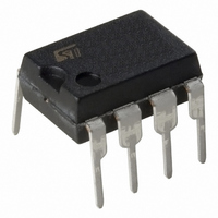
TL072IN STMicroelectronics, TL072IN Datasheet - Page 4

TL072IN
Manufacturer Part Number
TL072IN
Description
IC OP AMP JFET DUAL LNOISE 8-DIP
Manufacturer
STMicroelectronics
Specifications of TL072IN
Amplifier Type
J-FET
Number Of Circuits
2
Slew Rate
16 V/µs
Gain Bandwidth Product
4MHz
Current - Input Bias
20pA
Voltage - Input Offset
3000µV
Current - Supply
1.4mA
Current - Output / Channel
40mA
Voltage - Supply, Single/dual (±)
6 V ~ 36 V, ±3 V ~ 18 V
Operating Temperature
-40°C ~ 105°C
Mounting Type
Through Hole
Package / Case
8-DIP (0.300", 7.62mm)
Number Of Channels
2
Common Mode Rejection Ratio (min)
80 dB
Input Offset Voltage
10 mV
Input Bias Current (max)
200 pA
Supply Current
2.5 mA
Maximum Power Dissipation
680 mW
Maximum Operating Temperature
+ 105 C
Minimum Operating Temperature
- 40 C
Dual Supply Voltage
+/- 5 V, +/- 9 V, +/- 12 V, +/- 15 V
Maximum Dual Supply Voltage
+/- 18 V
Minimum Dual Supply Voltage
+/- 3 V
Mounting Style
Through Hole
Shutdown
No
Technology
BiFET
Voltage Gain Db
106.02 dB
Bandwidth
4 MHz
Channel Separation
120
Common Mode Rejection Ratio
86
Current, Input Bias
20 pA
Current, Input Offset
5 pA
Current, Output
20 mA
Current, Supply
1.4 mA
Harmonic Distortion
0.01 %
Number Of Amplifiers
Dual
Package Type
DIP-8
Resistance, Input
10^12 Ohms
Signal Gain
200 V/mV
Temperature, Operating, Range
-40 to +105 °C
Time, Rise
0.1 μs
Voltage, Input
±15 V
Voltage, Noise
15 nV/sqrt Hz
Voltage, Offset
3 mV
Voltage, Supply
6 to 36 V
Lead Free Status / RoHS Status
Lead free / RoHS Compliant
Output Type
-
-3db Bandwidth
-
Lead Free Status / Rohs Status
Lead free / RoHS Compliant
Other names
497-7659-5
TL072IN
TL072IN
00022-1,00053-1
Note2.
Note3.
Note4.
Note1. Marking of TDK part No, Date code, Country of origin.
TDK CORPORATION
1-2. Connector Configuration
Input side CN1
For circuit connection, please prefer to test circuit diagram [5].
Please use minimum of 2mm clearance (all directions) between inverter high voltage area and any conductors.
Please refer to mechanical drawing for marking of high voltage area.
Open voltage (strike voltage) is measured across the transformer secondary winding at no lo ad as the reading at
the output connector would be less than the actual value.
* : Conformity to RoHS Directive:This means that, in conformity with EU Directive 2002/95/EC,
Pin No.
CN1-1
CN1-2
CN1-3
CN1-4
CN1-5
lead, cadmium, hexavalent chromium, and specific bromi ne-based flame retardants, PBB
and PBDE, have not been used,except for exempted applications.
1) TDK part No., Date code, Country of origin, is marked on the transformer.
2) Date code example. (ex. APR. 2001, Revision No.A)
3) Country of origin code example. (ex. MADE IN JAPAN. MADE IN CHINA).
Symbols
GND
N.C.
Vin
CXA-L0505-NJL CXA-L0512-NJL CXA-L0524-NJL
Ratings
5
5V
0V
-
No.
7
PRODUCT DRAWING
NAME OF DRAWING
MATERIALS NAME
Ratings
12V
0V
R
-
Blank
One digit of production month. (Oct. : X , Nov. : Y, Dec. : Z).
Last digit of producti on year.
A
DC-AC INVERTER UNIT CXA-L05xx-NJL
Product Conforming to RoHS Directive* Identification sign
PRODUCT NAME or MODEL,TITLE
Ratings
24V
0V
Re vision No. (PWB Pattern change sample)
-
QU
The output side is isolated from the input side.
V
HIGH
MATERIAL
Output side CN2
Pin No.
CN2-1
CN2-2
CN2-3
DRAWING No.
is based on V
CTR-0732-E
TSB-08-01-05(00) form-6(A4)
Common in the Series
Symbols
V
V
N.C.
HIGH
LOW
LOW
.
600Vrms
Ratings
(0V)
REMARK
-
PAGE
3


