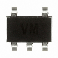
TS507IYLT STMicroelectronics, TS507IYLT Datasheet

TS507IYLT
Specifications of TS507IYLT
Available stocks
Related parts for TS507IYLT
TS507IYLT Summary of contents
Page 1
Features ■ Ultra low offset voltage: 25 µV typ, 100 µV max ■ Rail-to-rail input/output voltage swing ■ Operating from 2 5.5 V ■ High speed: 1.9 MHz ■ 45° phase margin with 100 pF ■ Low consumption: ...
Page 2
Contents Contents 1 Absolute maximum ratings and operating conditions . . . . . . . . . . . . . 3 2 Electrical characteristics . . . . . . . . . . . . . . ...
Page 3
TS507 1 Absolute maximum ratings and operating conditions Table 1. Absolute maximum ratings (AMR) Symbol V Supply voltage CC V Differential input voltage id V Input voltage in T Storage temperature stg Thermal resistance junction to ambient R SOT23-5 thja ...
Page 4
Electrical characteristics 2 Electrical characteristics Table 3. Electrical characteristics connected Symbol Parameter DC performance (2) V Input offset voltage io ΔV /Δt V drift vs. temperature Input bias current ib I ...
Page 5
TS507 Table 3. Electrical characteristics connected Symbol Parameter I sink I out I source I Supply current (per operator) CC Dynamic performance GBP Gain bandwidth product φ Phase margin m G Gain margin m ...
Page 6
Electrical characteristics Table 4. Electrical characteristics connected Symbol Parameter DC performance (2) V Input offset voltage io ΔV V drift vs. temperature Input bias current ib I Input offset current io ...
Page 7
TS507 Table 4. Electrical characteristics connected Symbol Parameter Dynamic performance GBP Gain bandwidth product φ Phase margin m G Gain margin m SR Slew rate e Equivalent input noise voltage N THD+e THD + ...
Page 8
Electrical characteristics Table 5. Electrical characteristics connected Symbol Parameter DC performance (2) V Input offset voltage io ΔV V drift vs. temperature Input bias current ib I Input offset current io ...
Page 9
TS507 Table 5. Electrical characteristics connected Symbol Parameter Dynamic performance GBP Gain bandwidth product φ Phase margin m G Gain margin m SR Slew rate e Equivalent input noise voltage N THD+e THD + ...
Page 10
Electrical characteristics Figure 1. Input offset voltage distribution for ≤ -1.2V at T=25°C icm CC 30 Vio distribution at T=25°C for 0V<=Vicm<=Vcc-1. -120 -100 -80 -60 -40 -20 0 Input offset voltage ...
Page 11
TS507 Figure 7. Supply current vs. input common mode voltage in closed loop configuration at V 1.0 1.0 0.8 0.7 T=-40°C 0.5 0.5 0.3 Vcc=5V Closed loop 0.2 0.0 0 Input common mode voltage ...
Page 12
Electrical characteristics Figure 13. Output current vs. output voltage at V =5V CC 150 T=25°C 125 100 100 75 T=125° Vcc= -25 -50 -75 Sink -100 -100 Vid=-1V -125 T=-40°C -150 0.0 0.0 1.0 1.0 2.0 ...
Page 13
TS507 Figure 19. Gain margin according the output load =5V and T=25°C CC 1E-6 1E-7 UNSTABLE 1E-8 1E-9 1E-10 1E- STABLE 1E- 100 1k Load Resistor ( Figure 21. Gain margin vs. output current, ...
Page 14
Electrical characteristics Figure 25. Distortion + noise vs. frequency 0.01 Vout=Vcc-1.5Vpp Rl=2kO ain=1 BW =80kHz Vicm =(Vcc-1V)/2 1E-3 1E-4 10 100 Frequency (Hz) 14/20 Figure 26. Noise vs. frequency 1000 100 Vcc=2.7V Vcc=3.3V 10 Vcc=5V 1000 10000 ...
Page 15
TS507 3 Application note An application note, based on the TS507, describes three compensation techniques for solving stability issues when driving large capacitive loads. Two of them are briefly explained here. For more details, refer to the application note on ...
Page 16
Application note 3.2 In-the-loop-compensation technique The second technique is called the in-the-loop-compensation technique, because the additional components (a resistor and a capacitor) used to improve the stability are inserted in the feedback loop (see Figure 30. In-the-loop compensation schematics This ...
Page 17
... These packages have a lead-free second level interconnect. The category of second level interconnect is marked on the package and on the inner box label, in compliance with JEDEC Standard JESD97. The maximum ratings related to soldering conditions are also marked on the inner box label. ECOPACK is an STMicroelectronics trademark. ECOPACK specifications are available at: www.st.com. 4.1 SOT23-5 package information Figure 31 ...
Page 18
Package information 4.2 SO-8 package Figure 32. SO-8 package mechanical drawing Table 8. SO-8 package mechanical data Ref ccc 18/20 Dimensions Millimeters Min. Typ. Max. 1.75 0.10 0.25 ...
Page 19
... Order code TS507ID TS507IDT (1) TS507IYD (1) TS507IYDT TS507ILT (1) TS507IYLT TS507CD TS507CDT TS507CLT 1. Qualification and characterization according to AEC Q100 and Q003 or equivalent, advanced screening according to AEC Q001 & Q 002 or equivalent are on-going. 2. All information related to the SOT23-5 package is subject to change without notice. 6 Revision history Table 10 ...
Page 20
... Information in this document is provided solely in connection with ST products. STMicroelectronics NV and its subsidiaries (“ST”) reserve the right to make changes, corrections, modifications or improvements, to this document, and the products and services described herein at any time, without notice. All ST products are sold pursuant to ST’s terms and conditions of sale. ...


