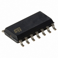
TSH73CDT STMicroelectronics, TSH73CDT Datasheet - Page 23

TSH73CDT
Manufacturer Part Number
TSH73CDT
Description
IC OP AMP TRIPLE LP WIDE 14-SOIC
Manufacturer
STMicroelectronics
Datasheet
1.TSH73CPT.pdf
(33 pages)
Specifications of TSH73CDT
Amplifier Type
General Purpose
Number Of Circuits
3
Output Type
Rail-to-Rail
Slew Rate
118 V/µs
Gain Bandwidth Product
65MHz
-3db Bandwidth
100MHz
Current - Input Bias
6µA
Voltage - Input Offset
800µV
Current - Supply
9.8mA
Current - Output / Channel
55mA
Voltage - Supply, Single/dual (±)
3 V ~ 12 V, ±1.5 V ~ 6 V
Operating Temperature
0°C ~ 70°C
Mounting Type
Surface Mount
Package / Case
14-SOIC (3.9mm Width), 14-SOL
Number Of Channels
3
Voltage Gain Db
84 dB
Common Mode Rejection Ratio (min)
72 dB
Input Offset Voltage
10 mV
Operating Supply Voltage
5 V, 9 V
Supply Current
31.5 mA
Maximum Operating Temperature
+ 70 C
Mounting Style
SMD/SMT
Maximum Dual Supply Voltage
+/- 6 V
Minimum Operating Temperature
0 C
Lead Free Status / RoHS Status
Lead free / RoHS Compliant
Other names
497-8155-2
TSH73CDT
TSH73CDT
Available stocks
Company
Part Number
Manufacturer
Quantity
Price
Part Number:
TSH73CDT
Manufacturer:
ST
Quantity:
20 000
TSH70,71,72,73,74,75
5.4
Table 7.
Precautions when operating on an asymmetrical supply
The TSH7X can be used with either a dual or a single supply. If a single supply is used, the
inputs are biased to the mid-supply voltage (+V
designed, in order to reject any noise present on the supply rail.
As the bias current is 15uA, you must carefully choose the resistance R1 so as not to
introduce an offset mismatch at the amplifier inputs.
Figure 49. Schematic of asymmetrical (single) supply
R1 = 10K Ω is a typical and convenient value. C1, C2, C3 are bypass capacitors that filter
perturbations on V
and C2 = C3 = 100uF.
R2, R3 are such that the current through them must be greater than 100 times the bias
current. Therefore, we set R2 = R3 = 4.7K Ω .
Diff Phase Step1
Diff Phase Step2
Diff Phase Step3
Diff Phase Step4
Diff Phase Step5
IN
Diff Gain Step1
Diff Gain Step2
Diff Gain Step3
Diff Gain Step4
Diff Gain Step5
Diff Phase pos
Diff Phase neg
Diff Phase pp
Parameter
C
R1
in
Video results
R2
R3 C1
CC
Vcc+
, as well as for the input and output signals. We choose C1 = 100nF
C2
C3
V
CC
R4
Value
+
-
-0.5
-0.7
-0.3
-0.1
-0.4
-0.2
-0.2
-0.1
-0.1
-0.2
=
0.2
0
0
R5
±
Cf
2.5V
C
out
CC
OUT
/2). This bias network must be carefully
R
L
V
CC
Value
-0.3
-0.6
-0.5
-0.3
-0.5
-0.4
-0.4
-0.4
-0.3
-0.1
0.1
0.5
0.1
=
±
5V
Testing Conditions
Unit
deg
deg
deg
deg
deg
deg
deg
deg
%
%
%
%
%
23/33


