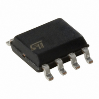
TL081IDT STMicroelectronics, TL081IDT Datasheet

TL081IDT
Specifications of TL081IDT
Available stocks
Related parts for TL081IDT
TL081IDT Summary of contents
Page 1
General purpose JFET single operational amplifiers Features ■ Wide common-mode ( differential voltage range ■ Low input bias and offset current ■ Output short-circuit protection ■ High input impedance JFET input stage ■ Internal frequency compensation ■ Latch-up ...
Page 2
Schematic diagram 1 Schematic diagram Figure 1. Schematic diagram V CC Non-inverting input Inverting input V CC Figure 2. Input offset voltage null circuit 2/15 30k 1.3k 1.3k 35k 35k Offset Null1 Offset Null2 TL081 N1 100k Ω ...
Page 3
TL081 2 Absolute maximum ratings Table 1. Absolute maximum ratings Symbol V Supply voltage CC V Input voltage in V Differential input voltage id P Power dissipation tot Output short-circuit duration T Storage temperature range stg Thermal resistance junction to ...
Page 4
Electrical characteristics 3 Electrical characteristics Table ±15V amb Symbol Parameter Input offset voltage ( +25°C amb V io ≤ T ≤ min amb max DV Input offset voltage drift io (1) ...
Page 5
TL081 Table ±15V amb Symbol Parameter Rise time (T = +25°C) amb 20mV 2kΩ Overshoot (T = +25°C) amb 20mV, R ...
Page 6
Electrical characteristics Figure 3. Maximum peak-to-peak output voltage versus frequency Figure 5. Maximum peak-to-peak output voltage versus frequency Figure 7. Maximum peak-to-peak output voltage versus load resistance 6/15 Figure 4. Maximum peak-to-peak output voltage versus frequency Figure 6. Maximum peak-to-peak ...
Page 7
TL081 Figure 9. Input bias current versus free air temperature 100 V 15V = 0.1 0.01 -50 - TEMPERATURE (˚C) Figure 11. Large signal differential voltage amplification and phase shift versus frequency W Figure 13. ...
Page 8
Electrical characteristics Figure 15. Common mode rejection ratio versus free air temperature kΩ 15V -75 -50 -25 0 TEMPERATURE (˚C) Figure 17. Output voltage versus ...
Page 9
TL081 4 Parameter measurement information Figure 20. Voltage follower Parameter measurement information Figure 21. Gain-of-10 inverting amplifier 10k Ω 1k Ω TL081 100pF L 9/15 ...
Page 10
Typical applications 5 Typical applications Figure 22. 0.5 Hz square wave oscillator Figure 23. High Q notch filter 10/ Ω 3.3k Ω +15V - TL0 Ω -15V C = 3.3 μF ...
Page 11
TL081 6 Package information In order to meet environmental requirements, ST offers these devices in ECOPACK® packages. These packages have a lead-free second level interconnect. The category of second level interconnect is marked on the package and on the inner ...
Page 12
Package information 6.1 DIP 8 package information Figure 24. DIP8 package mechanical drawing Table 4. DIP8 package mechanical data Ref 12/15 Dimensions Millimeters Min. Typ. Max. 5.33 ...
Page 13
TL081 6.2 SO-8 package information Figure 25. SO-8 package mechanical drawing Table 5. SO-8 package mechanical data Ref ccc Dimensions Millimeters Min. Typ. Max. 1.75 0.10 0.25 1.25 ...
Page 14
Ordering information 7 Ordering information Table 6. Order codes Order code TL081IN TL081AIN TL081BIN TL081ID/IDT TL081AID/AIDT TL081BID/BIDT (1) TL081IYD/DT (1) TL081AIYD/DT (1) TL081BIYD/DT TL081CN TL081ACN TL081BCN TL081CD/CDT TL081ACD/ACDT TL081BCD/BCDT 1. Qualification and characterization according to AEC Q100 and Q003 or ...
Page 15
... TL081 Information in this document is provided solely in connection with ST products. STMicroelectronics NV and its subsidiaries (“ST”) reserve the right to make changes, corrections, modifications or improvements, to this document, and the products and services described herein at any time, without notice. All ST products are sold pursuant to ST’s terms and conditions of sale. ...


