AD624BDZ Analog Devices Inc, AD624BDZ Datasheet - Page 9
AD624BDZ
Manufacturer Part Number
AD624BDZ
Description
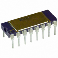
IC AMP INST 25MHZ PREC LN 16CDIP
Manufacturer
Analog Devices Inc
Datasheet
1.AD624ADZ.pdf
(16 pages)
Specifications of AD624BDZ
Amplifier Type
Instrumentation
Number Of Circuits
1
Slew Rate
5 V/µs
Gain Bandwidth Product
25MHz
-3db Bandwidth
1MHz
Current - Input Bias
25nA
Voltage - Input Offset
75µV
Current - Supply
3.5mA
Voltage - Supply, Single/dual (±)
±6 V ~ 18 V
Operating Temperature
-25°C ~ 85°C
Mounting Type
Through Hole
Package / Case
16-CDIP (0.300", 7.62mm)
No. Of Amplifiers
1
Input Offset Voltage
75µV
Gain Db Min
1dB
Bandwidth
25MHz
Amplifier Output
Single Ended
Cmrr
120dB
Supply Voltage Range
± 6V To ± 18V
Rohs Compliant
Yes
Lead Free Status / RoHS Status
Lead free / RoHS Compliant
Output Type
-
Current - Output / Channel
-
Available stocks
Company
Part Number
Manufacturer
Quantity
Price

Part Number:
AD624BDZ
Manufacturer:
ADI/亚德诺
Quantity:
20 000


NOISE
The AD624 is designed to provide noise performance near the
theoretical noise floor. This is an extremely important design
criteria as the front end noise of an instrumentation amplifier is
the ultimate limitation on the resolution of the data acquisition
system it is being used in. There are two sources of noise in an
instrument amplifier, the input noise, predominantly generated
by the differential input stage, and the output noise, generated
by the output amplifier. Both of these components are present
at the input (and output) of the instrumentation amplifier. At
the input, the input noise will appear unaltered; the output
noise will be attenuated by the closed loop gain (at the output,
the output noise will be unaltered; the input noise will be ampli-
fied by the closed loop gain). Those two noise sources must be
root sum squared to determine the total noise level expected at
the input (or output).
The low frequency (0.1 Hz to 10 Hz) voltage noise due to the
output stage is 10 µV p-p, the contribution of the input stage is
0.2 µV p-p. At a gain of 10, the RTI voltage noise would be
1 µV p-p,
10.2 µV p-p,
applications using either internal or external gain resistors.
INPUT BIAS CURRENTS
Input bias currents are those currents necessary to bias the input
transistors of a dc amplifier. Bias currents are an additional
source of input error and must be considered in a total error
budget. The bias currents when multiplied by the source resis-
tance imbalance appear as an additional offset voltage. (What is
of concern in calculating bias current errors is the change in bias
current with respect to signal voltage and temperature.) Input
offset current is the difference between the two input bias cur-
rents. The effect of offset current is an input offset voltage whose
magnitude is the offset current times the source resistance.
10
G
10
2
2
+ 0.2
+ 0.2 G
( )
(
( )
2
. The RTO voltage noise would be
AD624
AD624
)
–V
+V
2
–V
+V
S
. These calculations hold for
S
S
S
LOAD
LOAD
TO
POWER
SUPPLY
GROUND
TO
POWER
SUPPLY
GROUND
Although instrumentation amplifiers have differential inputs,
there must be a return path for the bias currents. If this is not
provided, those currents will charge stray capacitances, causing
the output to drift uncontrollably or to saturate. Therefore,
when amplifying “floating” input sources such as transformers
and thermocouples, as well as ac-coupled sources, there must
still be a dc path from each input to ground, (see Figure 31).
COMMON-MODE REJECTION
Common-mode rejection is a measure of the change in output
voltage when both inputs are changed by equal amounts. These
specifications are usually given for a full-range input voltage
change and a specified source imbalance. “Common-Mode
Rejection Ratio” (CMRR) is a ratio expression while “Common-
Mode Rejection” (CMR) is the logarithm of that ratio. For
example, a CMRR of 10,000 corresponds to a CMR of 80 dB.
In an instrumentation amplifier, ac common-mode rejection is
only as good as the differential phase shift. Degradation of ac
common-mode rejection is caused by unequal drops across
differing track resistances and a differential phase shift due to
varied stray capacitances or cable capacitances. In many appli-
cations shielded cables are used to minimize noise. This tech-
nique can create common-mode rejection errors unless the
shield is properly driven. Figures 32 and 33 shows active data
guards which are configured to improve ac common-mode
rejection by “bootstrapping” the capacitances of the input
cabling, thus minimizing differential phase shift.
100
100
100
AD712
AD711
–INPUT
G = 200
+INPUT
–V
AD624
RG
–INPUT
S
+INPUT
–V
+V
2
RG
RG
S
S
1
2
AD624
–V
+V
AD624
S
S
–V
+V
S
S
LOAD
≥
REFERENCE
TO
POWER
SUPPLY
GROUND
AD624
REFERENCE
V
OUT
V
OUT
Related parts for AD624BDZ
Image
Part Number
Description
Manufacturer
Datasheet
Request
R

Part Number:
Description:
±1.7g Dual-Axis IMEMS Accelerometer Evaluation Board
Manufacturer:
Analog Devices Inc
Datasheet:

Part Number:
Description:
Inertial Sensor Evaluation System
Manufacturer:
Analog Devices Inc
Datasheet:
Part Number:
Description:
Manufacturer:
Analog Devices Inc
Datasheet:
Part Number:
Description:
Manufacturer:
Analog Devices Inc
Datasheet:
Part Number:
Description:
Manufacturer:
Analog Devices Inc
Datasheet:
Part Number:
Description:
Manufacturer:
Analog Devices Inc
Datasheet:
Part Number:
Description:
Manufacturer:
Analog Devices Inc
Datasheet:
Part Number:
Description:
Manufacturer:
Analog Devices Inc
Datasheet:
Part Number:
Description:
Manufacturer:
Analog Devices Inc
Datasheet:
Part Number:
Description:
Manufacturer:
Analog Devices Inc
Datasheet:
Part Number:
Description:
Manufacturer:
Analog Devices Inc
Datasheet:
Part Number:
Description:
Manufacturer:
Analog Devices Inc
Datasheet:
Part Number:
Description:
Manufacturer:
Analog Devices Inc
Datasheet: