AD624BDZ Analog Devices Inc, AD624BDZ Datasheet - Page 8
AD624BDZ
Manufacturer Part Number
AD624BDZ
Description
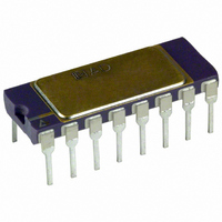
IC AMP INST 25MHZ PREC LN 16CDIP
Manufacturer
Analog Devices Inc
Datasheet
1.AD624ADZ.pdf
(16 pages)
Specifications of AD624BDZ
Amplifier Type
Instrumentation
Number Of Circuits
1
Slew Rate
5 V/µs
Gain Bandwidth Product
25MHz
-3db Bandwidth
1MHz
Current - Input Bias
25nA
Voltage - Input Offset
75µV
Current - Supply
3.5mA
Voltage - Supply, Single/dual (±)
±6 V ~ 18 V
Operating Temperature
-25°C ~ 85°C
Mounting Type
Through Hole
Package / Case
16-CDIP (0.300", 7.62mm)
No. Of Amplifiers
1
Input Offset Voltage
75µV
Gain Db Min
1dB
Bandwidth
25MHz
Amplifier Output
Single Ended
Cmrr
120dB
Supply Voltage Range
± 6V To ± 18V
Rohs Compliant
Yes
Lead Free Status / RoHS Status
Lead free / RoHS Compliant
Output Type
-
Current - Output / Channel
-
Available stocks
Company
Part Number
Manufacturer
Quantity
Price

Part Number:
AD624BDZ
Manufacturer:
ADI/亚德诺
Quantity:
20 000


AD624
directly proportional to gain i.e., input offset as measured at
the output at G = 100 is 100 times greater than at G = 1.
Output offset is independent of gain. At low gains, output offset
drift is dominant, while at high gains input offset drift domi-
nates. Therefore, the output offset voltage drift is normally
specified as drift at G = 1 (where input effects are insignificant),
while input offset voltage drift is given by drift specification at a
high gain (where output offset effects are negligible). All input-
related numbers are referred to the input (RTI) which is to say
that the effect on the output is “G” times larger. Voltage offset
vs. power supply is also specified at one or more gain settings
and is also RTI.
By separating these errors, one can evaluate the total error inde-
pendent of the gain setting used. In a given gain configura-
tion both errors can be combined to give a total error referred to
the input (R.T.I.) or output (R.T.O.) by the following formula:
As an illustration, a typical AD624 might have a +250 µV out-
put offset and a –50 µV input offset. In a unity gain configura-
tion, the total output offset would be 200 µV or the sum of the
two. At a gain of 100, the output offset would be –4.75 mV
or: +250 µV + 100 (–50 µV) = –4.75 mV.
The AD624 provides for both input and output offset adjust-
ment. This optimizes nulling in very high precision applications
and minimizes offset voltage effects in switched gain applica-
tions. In such applications the input offset is adjusted first at the
highest programmed gain, then the output offset is adjusted at
G = 1.
GAIN
The AD624 includes high accuracy pretrimmed internal
gain resistors. These allow for single connection program-
ming of gains of 1, 100, 200 and 500. Additionally, a variety
of gains including a pretrimmed gain of 1000 can be achieved
through series and parallel combinations of the internal resis-
tors. Table I shows the available gains and the appropriate
pin connections and gain temperature coefficients.
The gain values achieved via the combination of internal
resistors are extremely useful. The temperature coefficient of the
gain is dependent primarily on the mismatch of the temperature
coefficients of the various internal resistors. Tracking of these
resistors is extremely tight resulting in the low gain TCs shown
in Table I.
If the desired value of gain is not attainable using the inter-
nal resistors, a single external resistor can be used to achieve
any gain between 1 and 10,000. This resistor connected between
Total Error R.T.I. = input error + (output error/gain)
Total Error R.T.O. = (Gain × input error) + output error
–INPUT
+INPUT
G = 200
G = 500
G = 100
RG
RG
2
1
+V
AD624
S
–V
10k
S
INPUT
OFFSET
NULL
OUTPUT
SIGNAL
COMMON
V
OUT
Gain
(Nominal)
1
100
125
137
186.5
200
250
333
375
500
624
688
831
1000
Pins 3 and 16 programs the gain according to the formula
(see Figure 29). For best results R
tor with a low temperature coefficient. An external R
gain accuracy and gain drift due to the mismatch between it and
the internal thin-film resistors R56 and R57. Gain accuracy is
determined by the tolerance of the external R
accuracy of the internal resistors (±20%). Gain drift is determined
by the mismatch of the temperature coefficient of R
perature coefficient of the internal resistors (–15 ppm/°C typ),
and the temperature coefficient of the internal interconnections.
The AD624 may also be configured to provide gain in the out-
put stage. Figure 30 shows an H pad attenuator connected to
the reference and sense lines of the AD624. The values of R1,
R2 and R3 should be selected to be as low as possible to mini-
mize the gain variation and reduction of CMRR. Varying R2
will precisely set the gain without affecting CMRR. CMRR is
determined by the match of R1 and R3.
+INPUT
–INPUT
1k
1.5k
G =
–INPUT
+INPUT
G = 500
OR
(R
G = 100
G = 200
RG
2
||20k ) + R
0 ppm/°C
Temperature
Coefficient
(Nominal)
–0 ppm/°C
–1.5 ppm/°C
–5 ppm/°C
–5.5 ppm/°C
–6.5 ppm/°C
–3.5 ppm/°C
–5.5 ppm/°C
–15 ppm/°C
–0.5 ppm/°C
–10 ppm/°C
–5 ppm/°C
–1.5 ppm/°C
+4 ppm/°C
RG
2
(R
2.105k
1
2
||20k )
RG
RG
1
2
1
+ R
R
3
)
Table I.
G
AD624
=
–V
+V
G − 1
S
S
40k
AD624
G
–V
Pin 3
to Pin
–
13
13
13
13
12
12
12
12
11
11
11
11
11
+V
should be a precision resis-
S
S
(R
1
G =
+ R
G
2
40.000
2.105
R3
6k
R2
5k
+ R
and the absolute
6k
R1
Connect Pins
–
–
11 to 16
11 to 12
11 to 12 to 16
–
11 to 13
11 to 16
13 to 16
–
13 to 16
11 to 12; 13 to 16
16 to 12
16 to 12; 13 to 11
3
) || R
G
REFERENCE
+ 1 = 20
G
R
and the tem-
L
L
affects both
V
2k
OUT
V
20%
OUT
Related parts for AD624BDZ
Image
Part Number
Description
Manufacturer
Datasheet
Request
R

Part Number:
Description:
±1.7g Dual-Axis IMEMS Accelerometer Evaluation Board
Manufacturer:
Analog Devices Inc
Datasheet:

Part Number:
Description:
Inertial Sensor Evaluation System
Manufacturer:
Analog Devices Inc
Datasheet:
Part Number:
Description:
Manufacturer:
Analog Devices Inc
Datasheet:
Part Number:
Description:
Manufacturer:
Analog Devices Inc
Datasheet:
Part Number:
Description:
Manufacturer:
Analog Devices Inc
Datasheet:
Part Number:
Description:
Manufacturer:
Analog Devices Inc
Datasheet:
Part Number:
Description:
Manufacturer:
Analog Devices Inc
Datasheet:
Part Number:
Description:
Manufacturer:
Analog Devices Inc
Datasheet:
Part Number:
Description:
Manufacturer:
Analog Devices Inc
Datasheet:
Part Number:
Description:
Manufacturer:
Analog Devices Inc
Datasheet:
Part Number:
Description:
Manufacturer:
Analog Devices Inc
Datasheet:
Part Number:
Description:
Manufacturer:
Analog Devices Inc
Datasheet:
Part Number:
Description:
Manufacturer:
Analog Devices Inc
Datasheet: