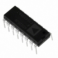
AD526JNZ Analog Devices Inc, AD526JNZ Datasheet - Page 4

AD526JNZ
Manufacturer Part Number
AD526JNZ
Description
IC AMP PGA 10MA 16DIP
Manufacturer
Analog Devices Inc
Type
Programmable Gain Amplifierr
Datasheet
1.AD526JNZ.pdf
(14 pages)
Specifications of AD526JNZ
Amplifier Type
Programmable Gain
Number Of Circuits
1
Slew Rate
24 V/µs
-3db Bandwidth
4MHz
Current - Input Bias
50pA
Voltage - Input Offset
400µV
Current - Supply
10mA
Current - Output / Channel
10mA
Voltage - Supply, Single/dual (±)
±4.5 V ~ 16.5 V
Operating Temperature
0°C ~ 70°C
Mounting Type
Through Hole
Package / Case
16-DIP (0.300", 7.62mm)
No. Of Amplifiers
1
Bandwidth
350kHz
No. Of Channels
1
Supply Voltage Range
± 4.5V To ± 16V
Amplifier Case Style
DIP
No. Of Pins
16
Operating Temperature Range
0°C To +70°C
Number Of Channels
1
Number Of Elements
1
Power Supply Requirement
Dual
Input Offset Voltage
1.5@±15VmV
Single Supply Voltage (typ)
Not RequiredV
Dual Supply Voltage (typ)
±5/±9/±12/±15V
Rail/rail I/o Type
No
Single Supply Voltage (min)
Not RequiredV
Single Supply Voltage (max)
Not RequiredV
Dual Supply Voltage (min)
±4.5V
Dual Supply Voltage (max)
±16.5V
Operating Temp Range
0C to 70C
Operating Temperature Classification
Commercial
Mounting
Through Hole
Pin Count
16
Package Type
PDIP
Lead Free Status / RoHS Status
Lead free / RoHS Compliant
Output Type
-
Gain Bandwidth Product
-
Lead Free Status / Rohs Status
Compliant
Available stocks
Company
Part Number
Manufacturer
Quantity
Price
AD526–Typical Performance Characteristics
Figure 1. Output Voltage Swing vs.
Supply Voltage, G = 16
Figure 7. Large Signal Frequency
Response
100nA
100pA
10nA
10pA
Figure 4. Input Bias Current vs.
Temperature
1nA
1pA
20
15
10
25
20
15
10
5
0
5
0
1k
–60
0
–20
SUPPLY VOLTAGE –
10k
5
GAIN = 1, 2, 4
TEMPERATURE – C
FREQUENCY – Hz
+25 C
R
L
20
= 2k
100k
10
60
GAIN = 8, 16
1M
15
V
100
10M
20
140
Figure 5. Input Bias Current vs. Input
Voltage
Figure 2. Output Voltage Swing vs.
Load Resistance
100
30
20
10
75
50
25
80
60
40
20
10
Figure 8. PSRR vs. Frequency
0
0
100
–10
1
10
LOAD RESISTANCE –
–5
INPUT VOLTAGE – V
FREQUENCY – Hz
100
–4–
–SUPPLY
1k
1k
0
V
@ V
SINE WAVE
S
15V WITH 1V p-p
=
10k
S
=
15V
5
+SUPPLY
15V
100k
10k
1M
10
1.0002
1.0001
1.0000
0.9999
0.9998
Figure 3. Input Bias Current vs.
Supply Voltage
Figure 9. Normalized Gain vs.
Temperature, Gain = 1
20
15
10
20
10
Figure 6. Gain vs. Frequency
1
5
0
10
0
–60
100
–20
SUPPLY VOLTAGE –
5
FREQUENCY – Hz
TEMPERATURE – C
1k
V
IN
= 0
20
10k
10
60
100k
V
15
4
16
100
1M
REV. D
2
8
1
10M
20
140


