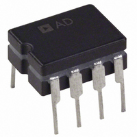
AD603AQ Analog Devices Inc, AD603AQ Datasheet - Page 13

AD603AQ
Manufacturer Part Number
AD603AQ
Description
IC AMP VGA 90MHZ LN 50MA 8CDIP
Manufacturer
Analog Devices Inc
Series
X-AMP®r
Specifications of AD603AQ
Rohs Status
RoHS non-compliant
Amplifier Type
Variable Gain
Number Of Circuits
1
Slew Rate
275 V/µs
-3db Bandwidth
90MHz
Current - Input Bias
200nA
Current - Supply
12.5mA
Current - Output / Channel
50mA
Voltage - Supply, Single/dual (±)
9.5 V ~ 12.6 V, ±4.75 V ~ 6.3 V
Operating Temperature
-40°C ~ 85°C
Mounting Type
Through Hole
Package / Case
8-CDIP (0.300", 7.62mm)
No. Of Amplifiers
1
Bandwidth
90MHz
Gain Accuracy
1.5dB
No. Of Channels
1
Supply Voltage Range
± 4.75V To ± 6.3V
Amplifier Case Style
DIP
No. Of Pins
8
Operating Temperature Range
-40°C To
Rohs Compliant
No
For Use With
AD603-EVALZ - BOARD EVALUATION FOR AD603
Output Type
-
Gain Bandwidth Product
-
Voltage - Input Offset
-
Lead Free Status / RoHS Status
Contains lead / RoHS non-compliant
Available stocks
Company
Part Number
Manufacturer
Quantity
Price
Part Number:
AD603AQ
Manufacturer:
ADI/亚德诺
Quantity:
20 000
output signal. The automatic gain control voltage, V
time integral of this error current. In order for V
thus the gain) to remain insensitive to short-term amplitude
fluctuations in the output signal, the rectified current in Q1 must,
on average, exactly balance the current in Q2. If the output of A2
is too small to do this, V
increase, until Q1 conducts sufficiently.
Consider the case where R8 is zero and the output voltage V
is a square wave at, say, 455 kHz, which is well above the corner
frequency of the control loop.
During the time V
of Q1, Q1 conducts; when V
the average collector current of Q1 is forced to be 300 mA, and
the square wave has a duty-cycle of 1:1, Q1’s collector current
when conducting must be 600 mA. With R8 omitted, the peak
amplitude of V
typically about 700 mV, or 2 V
therefore the amplitude at which the output stabilizes, has a
strong negative temperature coefficient (TC), typically
–1.7 mV/∞C. Although this may not be troublesome in some
applications, the correct value of R8 will render the output stable
with temperature.
To understand this, first note that the current in Q2 is made
to be proportional to absolute temperature (PTAT). For the
moment, continue to assume that the signal is a square wave.
When Q1 is conducting, V
voltage that is PTAT and which can be chosen to have an equal
but opposite TC to that of the V
than an application of the band gap voltage reference principle.
When R8 is chosen such that the sum of the voltage across it
and the V
V
of course, that Q1 and Q2 share the same thermal environment.
Since the average emitter current is 600 mA during each half-
cycle of the square wave, a resistor of 833 W would add a PTAT
REV. E
OUT
will be stable over a wide range of temperatures, provided,
BE
of Q1 is close to the band gap voltage of about 1.2 V,
OUT
OUT
is forced to be just the V
is negative with respect to the base voltage
AGC
OUT
will increase, causing the gain to
OUT
BE
BE
is now the sum of V
. This is actually nothing more
is positive, it is cut off. Since
peak-to-peak. This voltage,
BE
of Q1 at 600 mA,
AGC
BE
AGC
(and
and a
, is the
OUT
–13–
voltage of 500 mV at 300 K, increasing by 1.66 mV/∞C. In prac-
tice, the optimum value will depend on the type of transistor
used and, to a lesser extent, on the waveform for which the
temperature stability is to be optimized; for the inexpensive
2N3904/2N3906 pair and sine wave signals, the recommended
value is 806 W.
This resistor also serves to lower the peak current in Q1 when
more typical signals (usually sinusoidal) are involved, and the
1.8 kHz LP filter it forms with C
due to ripple in V
sine wave conditions will be higher than for a square wave, since
the average value of the current for an ideal rectifier would be
0.637 times as large, causing the output amplitude to be
1.88 (= 1.2/0.637) V, or 1.33 V rms. In practice, the somewhat
nonideal rectifier results in the sine wave output being regulated
to about 1.4 V rms, or 3.6 V p-p.
The bandwidth of the circuit exceeds 40 MHz. At 10.7 MHz,
the AGC threshold is 100 mV (–67 dBm) and its maximum gain
is 83 dB (20 log 1.4 V/100 mV). The circuit holds its output at
1.4 V rms for inputs as low as –67 dBm to +15 dBm (82 dB),
where the input signal exceeds the AD603’s maximum input
rating. For a 30 dBm input at 10.7 MHz, the second harmonic
is 34 dB down from the fundamental and the third harmonic is
35 dB down.
CAUTION
Careful component selection, circuit layout, power-supply
decoupling, and shielding are needed to minimize the AD603’s
susceptibility to interference from signals such as those from
radio and TV stations. In bench evaluation, we recommend
placing all of the components into a shielded box and using
feedthrough decoupling networks for the supply voltage. Circuit
layout and construction are also critical, since stray capacitances
and lead inductances can form resonant circuits and are a
potential source of circuit peaking, oscillation, or both.
AGC
. Note that the output amplitude under
AV
helps to minimize distortion
AD603


