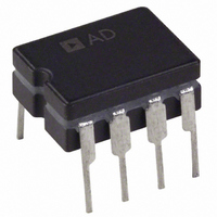
AD603AQ Analog Devices Inc, AD603AQ Datasheet - Page 12

AD603AQ
Manufacturer Part Number
AD603AQ
Description
IC AMP VGA 90MHZ LN 50MA 8CDIP
Manufacturer
Analog Devices Inc
Series
X-AMP®r
Specifications of AD603AQ
Rohs Status
RoHS non-compliant
Amplifier Type
Variable Gain
Number Of Circuits
1
Slew Rate
275 V/µs
-3db Bandwidth
90MHz
Current - Input Bias
200nA
Current - Supply
12.5mA
Current - Output / Channel
50mA
Voltage - Supply, Single/dual (±)
9.5 V ~ 12.6 V, ±4.75 V ~ 6.3 V
Operating Temperature
-40°C ~ 85°C
Mounting Type
Through Hole
Package / Case
8-CDIP (0.300", 7.62mm)
No. Of Amplifiers
1
Bandwidth
90MHz
Gain Accuracy
1.5dB
No. Of Channels
1
Supply Voltage Range
± 4.75V To ± 6.3V
Amplifier Case Style
DIP
No. Of Pins
8
Operating Temperature Range
-40°C To
Rohs Compliant
No
For Use With
AD603-EVALZ - BOARD EVALUATION FOR AD603
Output Type
-
Gain Bandwidth Product
-
Voltage - Input Offset
-
Lead Free Status / RoHS Status
Contains lead / RoHS non-compliant
Available stocks
Company
Part Number
Manufacturer
Quantity
Price
Part Number:
AD603AQ
Manufacturer:
ADI/亚德诺
Quantity:
20 000
AD603
–0.5
–1.0
–1.5
–2.0
–2.5
–3.0
J1
90
85
80
75
70
65
60
55
50
3.0
2.5
2.0
1.5
1.0
0.5
0.0
Figure 13. Gain Error for Cascaded Stages—
Low Ripple Mode
–0.2
–0.1
NOTES
1
2
R
C3 AND C5 ARE TANTALUM
T
Figure 14. ISNR vs. Control Voltage—
Low Ripple Mode
+
0.0
PROVIDES A 50
C3
100 F
RT
100
0
0.1
2
0.1 F
1
C1
0.2
2.49k
0.2
C4
0.1 F
0.3
R1
10V
INPUT IMPEDANCE
0.1 F
R2
2.49k
0.4
0.4
C7
V
0.5
V
C
C
5.49k
AD603
10V
R5
0.6
A1
0.6
0.7
5.5V
0.8
2.49k
0.8 0.9
R13
+
Figure 15. A Low Noise AGC Amplifier
C5
100 F
1.0
2
SEQUENTIAL GAIN
0.1 F
1V OFFSET FOR
1.0 1.1
C2
2.49k
C6
0.1 F
1.2
1.05k
R6
R3
10V
0.1 F
R4
2.49k
C8
–12–
AD603
10V
A2
THEORY OF THE AD603
A Low Noise AGC Amplifier
Figure 15 shows the ease with which the AD603 can be connected
as an AGC amplifier. The circuit illustrates many of the points
previously discussed: It uses few parts, has linear-in-dB gain,
operates from a single supply, uses two cascaded amplifiers in
sequential gain mode for maximum S/N ratio, and an external
resistor programs each amplifier’s gain. It also uses a simple
temperature-compensated detector.
The circuit operates from a single 10 V supply. Resistors R1,
R2, R3, and R4 bias the common pins of A1 and A2 at 5 V.
This pin is a low impedance point and must have a low impedance
path to ground, here provided by the 100 mF tantalum capacitors
and the 0.1 mF ceramic capacitors.
The cascaded amplifiers operate in sequential gain. Here, the
offset voltage between the Pin 2 (GNEG) of A1 and A2 is
1.05 V (42.14 dB ¥ 25 mV/dB), provided by a voltage divider
consisting of resistors R5, R6, and R7. Using standard values,
the offset is not exact, but it is not critical for this application.
The gain of both A1 and A2 is programmed by resistors R13
and R14, respectively, to be about 42 dB; thus the maximum
gain of the circuit is twice that, or 84 dB. The gain-control
range can be shifted up by as much as 20 dB by appropriate
choices of R13 and R14.
The circuit operates as follows. A1 and A2 are cascaded.
Capacitor C1 and the 100 W of resistance at the input of A1
form a time constant of 10 ms. C2 blocks the small dc offset
voltage at the output of A1 (which might otherwise saturate A2
at its maximum gain) and introduces a high-pass corner at about
16 kHz, eliminating low frequency noise.
A half-wave detector is used, based on Q1 and R8. The current
into capacitor C
current of Q2 (biased to be 300 mA at 300 K, 27∞C) and the col-
lector current of Q1, which increases with the amplitude of the
THIS CAPACITOR SETS
AGC TIME CONSTANT
6.5V
2.49k
R14
3.48k
R7
AGC LINE
0.1 F
C
AV
AV
10V
V
is just the difference between the collector
AGC
2N3906
2N3904
1.54k
806
Q2
Q1
R9
R8
10V
R10
1.24k
R11
3.83k
5V
R12
4.99k
0.1 F
C10
C11
0.1 F
C9
0.1 F
J2
REV. E


