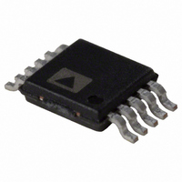
AD8250ARMZ Analog Devices Inc, AD8250ARMZ Datasheet - Page 15

AD8250ARMZ
Manufacturer Part Number
AD8250ARMZ
Description
IC AMP INST ICMOS LDRIFT 10MSOP
Manufacturer
Analog Devices Inc
Series
iCMOS®r
Type
Instrumentation Amplifierr
Datasheet
1.AD8250-EVALZ.pdf
(24 pages)
Specifications of AD8250ARMZ
Amplifier Type
Instrumentation
Number Of Circuits
1
Output Type
Push-Pull
Slew Rate
25 V/µs
-3db Bandwidth
10MHz
Current - Input Bias
5nA
Voltage - Input Offset
70µV
Current - Supply
4.1mA
Current - Output / Channel
37mA
Voltage - Supply, Single/dual (±)
10 V ~ 30 V, ±5 V ~ 15 V
Operating Temperature
-40°C ~ 85°C
Mounting Type
Surface Mount
Package / Case
10-MSOP, Micro10™, 10-uMAX, 10-uSOP
No. Of Amplifiers
1
Gain Db Min
1dB
Gain Db Max
10dB
Bandwidth
10MHz
Amplifier Output
Single Ended
Cmrr
110dB
Supply Voltage Range
± 5V To ± 15V
Supply Current
4.1mA
Rohs Compliant
Yes
Number Of Channels
1
Number Of Elements
3
Power Supply Requirement
Dual
Common Mode Rejection Ratio
80dB
Voltage Gain Db
20dB
Input Bias Current
0.03@±15VnA
Single Supply Voltage (typ)
Not RequiredV
Dual Supply Voltage (typ)
±9/±12V
Rail/rail I/o Type
No
Single Supply Voltage (min)
Not RequiredV
Single Supply Voltage (max)
Not RequiredV
Dual Supply Voltage (min)
±5V
Dual Supply Voltage (max)
±15V
Operating Temp Range
-40C to 85C
Operating Temperature Classification
Industrial
Mounting
Surface Mount
Pin Count
10
Package Type
MSOP
For Use With
AD8250-EVALZ - BOARD EVALUATION AD8250
Lead Free Status / RoHS Status
Lead free / RoHS Compliant
Gain Bandwidth Product
-
Lead Free Status / Rohs Status
Compliant
Available stocks
Company
Part Number
Manufacturer
Quantity
Price
Company:
Part Number:
AD8250ARMZ
Manufacturer:
MICROCHIP
Quantity:
21 500
Part Number:
AD8250ARMZ
Manufacturer:
ADI/亚德诺
Quantity:
20 000
Part Number:
AD8250ARMZ-RL
Manufacturer:
ADI/亚德诺
Quantity:
20 000
THEORY OF OPERATION
The AD8250 is a monolithic instrumentation amplifier based
on the classic, 3-op-amp topology as shown in Figure 47. It is
fabricated on the Analog Devices, Inc., proprietary iCMOS®
process that provides precision, linear performance, and a
robust digital interface. A parallel interface allows users to
digitally program gains of 1, 2, 5, and 10. Gain control is achieved
by switching resistors in an internal, precision resistor array (as
shown in Figure 47). Although the AD8250 has a voltage feedback
topology, the gain bandwidth product increases for gains of 1, 2,
and 5 because each gain has its own frequency compensation.
This results in maximum bandwidth at higher gains.
All internal amplifiers employ distortion cancellation circuitry
and achieve high linearity and ultralow THD. Laser trimmed
resistors allow for a maximum gain error of less than 0.03%
for G = 1 and minimum CMRR of 98 dB for G = 10. A pinout
optimized for high CMRR over frequency enables the AD8250
to offer a guaranteed minimum CMRR over frequency of 80 dB
at 50 kHz (G = 1). The balanced input reduces the parasitics
that, in the past, adversely affected CMRR performance.
GAIN SELECTION
Logic low and logic high voltage limits are listed in the
Specifications section. Typically, logic low is 0 V and logic high
is 5 V; both voltages are measured with respect to DGND. See
Table 2 for the permissible voltage range of DGND. The gain of
the AD8250 can be set using two methods.
+IN
–IN
2.2kΩ
2.2kΩ
+V
+V
–V
–V
S
S
S
S
A1
A2
WR
DIGITAL
GAIN
CONTROL
A0
Figure 47. Simplified Schematic
+V
+V
–V
–V
S
S
S
S
Rev. B | Page 15 of 24
2.2kΩ
2.2kΩ
+V
–V
+V
–V
10kΩ
10kΩ
S
S
S
S
Transparent Gain Mode
The easiest way to set the gain is to program it directly via a
logic high or logic low voltage applied to A0 and A1. Figure 48
shows an example of this gain setting method, referred to through-
out the data sheet as transparent gain mode. Tie WR to the negative
supply to engage transparent gain mode. In this mode, any change
in voltage applied to A0 and A1 from logic low to logic high, or
vice versa, immediately results in a gain change.
truth table for transparent gain mode, and
AD8250 configured in transparent gain mode.
A1
DGND
Figure 48. Transparent Gain Mode, A0 and A1 = High, G = 10
A3
NOTE:
1. IN TRANSPARENT GAIN MODE, WR IS TIED TO −V
10kΩ
10kΩ
THE VOLTAGE LEVELS ON A0 AND A1 DETERMINE
THE GAIN. IN THIS EXAMPLE, BOTH A0 AND A1 ARE
SET TO LOGIC HIGH, RESULTING IN A GAIN OF 10.
–IN
+IN
10μF
10μF
+V
–V
+V
–V
0.1µF
0.1µF
S
S
S
S
OUT
REF
+15V
–15V
AD8250
DGND
WR
A1
A0
REF
DGND
Figure 48
–15V
+5V
+5V
G = 10
S
Table 5
.
shows the
AD8250
is the


