OP462GSZ Analog Devices Inc, OP462GSZ Datasheet - Page 5
OP462GSZ
Manufacturer Part Number
OP462GSZ
Description
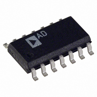
IC OPAMP GP R-R 15MHZ LN 14SOIC
Manufacturer
Analog Devices Inc
Type
General Purpose Amplifierr
Datasheet
1.OP162GSZ.pdf
(20 pages)
Specifications of OP462GSZ
Slew Rate
13 V/µs
Amplifier Type
General Purpose
Number Of Circuits
4
Output Type
Rail-to-Rail
Gain Bandwidth Product
15MHz
Current - Input Bias
260nA
Voltage - Input Offset
25µV
Current - Supply
550µA
Current - Output / Channel
30mA
Voltage - Supply, Single/dual (±)
2.7 V ~ 12 V, ±1.35 V ~ 6 V
Operating Temperature
-40°C ~ 125°C
Mounting Type
Surface Mount
Package / Case
14-SOIC (3.9mm Width), 14-SOL
Op Amp Type
Low Power
No. Of Amplifiers
4
Bandwidth
15MHz
Supply Voltage Range
2.7V To 12V
Amplifier Case Style
SOIC
No. Of Pins
14
Rail/rail I/o Type
Rail to Rail Output
Number Of Elements
4
Unity Gain Bandwidth Product
15MHz
Common Mode Rejection Ratio
70dB
Input Offset Voltage
325uV
Input Bias Current
600nA
Single Supply Voltage (typ)
3/5/9V
Dual Supply Voltage (typ)
±3/±5V
Voltage Gain In Db
98.89dB
Power Supply Rejection Ratio
120dB
Power Supply Requirement
Single/Dual
Shut Down Feature
No
Single Supply Voltage (min)
2.7V
Single Supply Voltage (max)
12V
Dual Supply Voltage (min)
±1.35V
Dual Supply Voltage (max)
±6V
Technology
BiCOM
Operating Temp Range
-40C to 125C
Operating Temperature Classification
Automotive
Mounting
Surface Mount
Pin Count
14
Package Type
SOIC N
Lead Free Status / RoHS Status
Lead free / RoHS Compliant
-3db Bandwidth
-
Lead Free Status / Rohs Status
Compliant
Available stocks
Company
Part Number
Manufacturer
Quantity
Price

Part Number:
OP462GSZ
Manufacturer:
ADI/亚德诺
Quantity:
20 000
Part Number:
OP462GSZ-REEL
Manufacturer:
ADI/亚德诺
Quantity:
20 000
Part Number:
OP462GSZ-REEL7
Manufacturer:
ADI/亚德诺
Quantity:
20 000


@ V
Table 3. Electrical Characteristics
Parameter
INPUT CHARACTERISTICS
OUTPUT CHARACTERISTICS
POWER SUPPLY
DYNAMIC PERFORMANCE
NOISE PERFORMANCE
1
2
Long-term offset voltage is guaranteed by a 1000 hour life test performed on three independent lots at +125°C, with an LTPD of 1.3.
Offset voltage drift is the average of the −40°C to +25°C delta and the +25°C to +125°C delta.
Offset Voltage
Input Bias Current
Input Offset Current
Input Voltage Range
Common-Mode Rejection
Large Signal Voltage Gain
Long-Term Offset Voltage
Offset Voltage Drift
Bias Current Drift
Output Voltage Swing High
Output Voltage Swing Low
Short-Circuit Current
Maximum Output Current
Power Supply Rejection Ratio
Supply Current/Amplifier
Supply Voltage Range
Slew Rate
Settling Time
Gain Bandwidth Product
Phase Margin
Voltage Noise
Voltage Noise Density
Current Noise Density
S
= ±5.0 V, V
CM
= 0 V, T
2
A
1
= 25°C, unless otherwise noted.
Symbol
V
I
I
V
CMRR
A
V
∆V
∆I
V
V
I
I
PSRR
I
V
SR
t
GBP
φ
e
e
i
B
OS
SC
OUT
SY
n
S
n
n
OS
CM
OS
OH
OL
S
VO
m
B
p-p
OS
/∆T
/∆T
Conditions
OP162G, OP262G, OP462G
−40°C ≤ T
H grade, –40°C ≤ T
D grade
−40°C ≤ T
−40°C ≤ T
−40°C ≤ T
−4.9 V ≤ V
R
R
−40°C ≤ T
G grade
I
I
I
I
Short to ground
V
−40°C ≤ T
OP162, V
−40°C ≤ T
OP262, OP462, V
−40°C ≤ T
−4 V < V
To 0.1%, A
0.1 Hz to 10 Hz
f = 1 kHz
f = 1 kHz
L
L
L
L
L
L
= 5 mA
= 5 mA
S
= 250 µA, –40°C ≤ T
= 250 µA, –40°C ≤ T
= 2 kΩ, –4.5 V ≤ V
= 10 kΩ, –4.5 V ≤ V
= ±1.35 V to ±6 V,
OUT
OUT
A
A
A
A
A
A
A
A
CM
Rev. F | Page 5 of 20
V
≤ +125°C
≤ +125°C
≤ +125°C
≤ +125°C
≤ +125°C
≤ +125°C
≤ +125°C
≤ +125°C
< 4 V, R
= –1, V
= 0 V
≤ +4.0 V, –40°C ≤ T
OUT
A
O
L
≤ +125°C
OUT
= 0 V
= 10 kΩ
= 2 V step
OUT
A
A
≤ +125°C
≤ +125°C
≤ +4.5 V
≤ +4.5 V
A
≤ +125°C
Min
–5
70
75
25
4.95
4.85
60
3.0 (±1.5)
OP162/OP262/OP462
Typ
25
0.8
260
±2.5
110
35
120
1
250
4.99
4.94
–4.99
–4.94
±80
±30
110
650
550
13
475
15
64
0.5
9.5
0.4
Max
325
800
1
3
5
500
650
±25
±40
+4
600
–4.95
–4.85
800
1.15
775
1
12 (±6)
Unit
µV
µV
mV
mV
mV
nA
nA
nA
nA
V
dB
V/mV
V/mV
V/mV
µV
µV/°C
pA/°C
V
V
V
V
mA
mA
dB
µA
mA
µA
mA
V
V/µs
ns
MHz
Degrees
µV p-p
nV/√ Hz
pA/√ Hz
Related parts for OP462GSZ
Image
Part Number
Description
Manufacturer
Datasheet
Request
R

Part Number:
Description:
±1.7g Dual-Axis IMEMS Accelerometer Evaluation Board
Manufacturer:
Analog Devices Inc
Datasheet:

Part Number:
Description:
Inertial Sensor Evaluation System
Manufacturer:
Analog Devices Inc
Datasheet:
Part Number:
Description:
Manufacturer:
Analog Devices Inc
Datasheet:
Part Number:
Description:
Manufacturer:
Analog Devices Inc
Datasheet:
Part Number:
Description:
Manufacturer:
Analog Devices Inc
Datasheet:
Part Number:
Description:
Manufacturer:
Analog Devices Inc
Datasheet:
Part Number:
Description:
Manufacturer:
Analog Devices Inc
Datasheet:
Part Number:
Description:
Manufacturer:
Analog Devices Inc
Datasheet:
Part Number:
Description:
Manufacturer:
Analog Devices Inc
Datasheet:
Part Number:
Description:
Manufacturer:
Analog Devices Inc
Datasheet:
Part Number:
Description:
Manufacturer:
Analog Devices Inc
Datasheet:
Part Number:
Description:
Manufacturer:
Analog Devices Inc
Datasheet:
Part Number:
Description:
Manufacturer:
Analog Devices Inc
Datasheet: