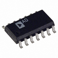
OP462GSZ Analog Devices Inc, OP462GSZ Datasheet - Page 13

OP462GSZ
Manufacturer Part Number
OP462GSZ
Description
IC OPAMP GP R-R 15MHZ LN 14SOIC
Manufacturer
Analog Devices Inc
Type
General Purpose Amplifierr
Datasheet
1.OP162GSZ.pdf
(20 pages)
Specifications of OP462GSZ
Slew Rate
13 V/µs
Amplifier Type
General Purpose
Number Of Circuits
4
Output Type
Rail-to-Rail
Gain Bandwidth Product
15MHz
Current - Input Bias
260nA
Voltage - Input Offset
25µV
Current - Supply
550µA
Current - Output / Channel
30mA
Voltage - Supply, Single/dual (±)
2.7 V ~ 12 V, ±1.35 V ~ 6 V
Operating Temperature
-40°C ~ 125°C
Mounting Type
Surface Mount
Package / Case
14-SOIC (3.9mm Width), 14-SOL
Op Amp Type
Low Power
No. Of Amplifiers
4
Bandwidth
15MHz
Supply Voltage Range
2.7V To 12V
Amplifier Case Style
SOIC
No. Of Pins
14
Rail/rail I/o Type
Rail to Rail Output
Number Of Elements
4
Unity Gain Bandwidth Product
15MHz
Common Mode Rejection Ratio
70dB
Input Offset Voltage
325uV
Input Bias Current
600nA
Single Supply Voltage (typ)
3/5/9V
Dual Supply Voltage (typ)
±3/±5V
Voltage Gain In Db
98.89dB
Power Supply Rejection Ratio
120dB
Power Supply Requirement
Single/Dual
Shut Down Feature
No
Single Supply Voltage (min)
2.7V
Single Supply Voltage (max)
12V
Dual Supply Voltage (min)
±1.35V
Dual Supply Voltage (max)
±6V
Technology
BiCOM
Operating Temp Range
-40C to 125C
Operating Temperature Classification
Automotive
Mounting
Surface Mount
Pin Count
14
Package Type
SOIC N
Lead Free Status / RoHS Status
Lead free / RoHS Compliant
-3db Bandwidth
-
Lead Free Status / Rohs Status
Compliant
Available stocks
Company
Part Number
Manufacturer
Quantity
Price
Part Number:
OP462GSZ
Manufacturer:
ADI/亚德诺
Quantity:
20 000
Part Number:
OP462GSZ-REEL
Manufacturer:
ADI/亚德诺
Quantity:
20 000
Part Number:
OP462GSZ-REEL7
Manufacturer:
ADI/亚德诺
Quantity:
20 000
and V
30 mA. For single 5 V supply applications, resistors less than
169 Ω are not recommended.
INPUT OVERVOLTAGE PROTECTION
The input voltage should be limited to ±6 V, or damage to the
device can occur. Electrostatic protection diodes placed in the
input stage of the device help protect the amplifier from static
discharge. Diodes are connected between each input as well as
from each input to both supply pins as shown in the simplified
equivalent circuit in Figure 33. If an input voltage exceeds either
supply voltage by more than 0.6 V, or if the differential input
voltage is greater than 0.6 V, these diodes energize causing
overvoltage damage.
The input current should be limited to less than 5 mA to
prevent degradation or destruction of the device by placing an
external resistor in series with the input at risk of being overdriven.
The size of the resistor can be calculated by dividing the maxi-
mum input voltage by 5 mA. For example, if the differential
input voltage could reach 5 V, the external resistor should be
5 V/5 mA = 1 kΩ. In practice, this resistor should be placed in
series with both inputs to balance any offset voltages created by
the input bias current.
OUTPUT PHASE REVERSAL
The OP162/OP262/OP462 are immune to phase reversal as
long as the input voltage is limited to ±6 V. Figure 30 shows the
output of a device with the input voltage driven beyond the
supply voltages. Although the device’s output does not change
phase, large currents due to input overvoltage could result,
damaging the device. In applications where the possibility of an
input voltage exceeding the supply voltage exists, overvoltage
protection should be used, as described in the previous section.
POWER DISSIPATION
The maximum power that can be safely dissipated by the
OP162/OP262/OP462 is limited by the associated rise in
junction temperature. The maximum safe junction temperature
is 150°C; device performance suffers when this limit is
exceeded. If this maximum is only momentarily exceeded,
proper circuit operation will be restored as soon as the die
temperature is reduced. Leaving the device in an “overheated”
condition for an extended period can result in permanent
damage to the device.
IN
swings up to 5 V, the output current will not exceed
V
IN
Figure 35. Output Short-Circuit Protection
OPx62
5V
169Ω
V
OUT
Rev. F | Page 13 of 20
To calculate the internal junction temperature of the OPx62, use
the formula
where:
T
P
θ
ambient temperature.
T
The power dissipated by the device can be calculated as
where:
I
V
V
Figure 36 and Figure 37 provide a convenient way to determine
if the device is being overheated. The maximum safe power
dissipation can be found graphically, based on the package type
and the ambient temperature around the package. By using the
previous equation, it is a simple matter to see if P
device’s power derating curve. To ensure proper operation, it is
important to observe the recommended derating curves shown
in Figure 36 and Figure 37.
LOAD
JA
DISS
J
A
S
OUT
is the OPx62 junction temperature.
is the OPx62 supply voltage.
is the ambient temperature of the circuit.
is the OPx62 package thermal resistance, junction-to-
T
is the OPx62 power dissipation.
P
is the OPx62 output load current.
is the OPx62 output voltage.
J
DISS
= P
Figure 36. Maximum Power Dissipation vs. Temperature for
0.9
0.8
0.7
0.6
0.5
0.4
0.3
0.2
0.1
0
= I
20
DISS
8-LEAD MSOP
LOAD
× θ
× (V
JA
40
+ T
8-LEAD TSSOP
S
– V
A
8-Lead Package Types
AMBIENT TEMPERATURE (°C)
8-LEAD SOIC
OUT
60
)
OP162/OP262/OP462
80
100
DISS
exceeds the
120


