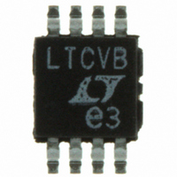
LTC6102HVCMS8#PBF Linear Technology, LTC6102HVCMS8#PBF Datasheet - Page 19

LTC6102HVCMS8#PBF
Manufacturer Part Number
LTC6102HVCMS8#PBF
Description
IC AMP CURRENT SENSE 8-MSOP
Manufacturer
Linear Technology
Datasheet
1.LTC6102CDDPBF.pdf
(26 pages)
Specifications of LTC6102HVCMS8#PBF
Amplifier Type
Current Sense
Number Of Circuits
1
Gain Bandwidth Product
200kHz
Current - Input Bias
60pA
Voltage - Input Offset
3µV
Current - Supply
420µA
Current - Output / Channel
1mA
Voltage - Supply, Single/dual (±)
5 V ~ 100 V
Operating Temperature
0°C ~ 70°C
Mounting Type
Surface Mount
Package / Case
8-MSOP, Micro8™, 8-uMAX, 8-uSOP,
Lead Free Status / RoHS Status
Lead free / RoHS Compliant
Output Type
-
-3db Bandwidth
-
Slew Rate
-
Available stocks
Company
Part Number
Manufacturer
Quantity
Price
If the output current is very low and an input transient
occurs, there may be a delay before the output voltage
begins changing. This can be reduced by increasing the
minimum output current, either by increasing R
decreasing R
is illustrated in the step response curves in the Typical
Performance Characteristics section of this datasheet.
Note that the curves are labeled with respect to the initial
output currents.
The speed is also affected by the external circuit. In this
case, if the input changes very quickly, the internal ampli-
fi er will slew the gate of the internal output FET (Figure 1)
in order to close the internal loop. This results in current
fl owing through R
rate will be determined by the amplifi er and FET charac-
teristics as well as the input resistor, R
R
decreasing the response time at the output. This will also
have the effect of increasing the maximum output current.
Using a larger R
since V
R
gain of the circuit.
Bandwidth
For applications that require higher bandwidth from the
LTC6102, care must be taken in choosing R
eral-purpose op-amp, the gain-bandwidth product is used
to determine the speed at a given gain. Gain is determined
by external resistors, and the gain-bandwidth product is
an intrinsic property of the amplifi er. The same is true
for the LTC6102, except that the feedback resistance is
determined by an internal FET characteristic. The feedback
impedance is approximately 1/g
The impedance is reduced as current into –INF is increased.
At 1mA, the impedance of the MOSFET is on the order of
10kΩ. R
as 1/(R
(R
This is illustrated in the characteristic curves, where gain
vs frequency for two input conditions is shown. The exact
impedance of the MOSFET is diffi cult to determine, as it
is a function of input current, process, and capacitance,
APPLICATIONS INFORMATION
IN
OUT
IN
will allow the output current to increase more quickly,
• g
will both have the effect of increasing the voltage
IN
OUT
m
IN
), with a maximum bandwidth of around 2MHz.
• g
sets the closed-loop gain of the internal loop
= I
m
IN
). The bandwidth is then limited to GBW •
OUT
. The effect of increased output current
OUT
IN
• R
and the internal FET. This current slew
will also decrease the response time,
OUT
. Reducing R
m
of the internal MOSFET.
IN
IN
. Using a smaller
and increasing
IN
. For a gen-
SENSE
or
and has a very different characteristic for low currents
vs high currents. However, it is clear that smaller values
of R
lower closed-loop bandwidth. V
chosen to maximize both I
highest speed. Theoretically, maximum bandwidth would
be achieved for the case where V
giving I
this may not be possible in a practical application. Note
that the MOSFET g
value of I
small AC input will help increase the bandwidth.
V
The LTC6102 has an internally regulated supply near V+
for internal bias. It is not intended for use as a supply or
bias pin for external circuitry. A 0.1μF capacitor should be
connected between the V
should be located very near to the LTC6102 for the best
performance. In applications which have large supply tran-
sients, a 6.8V zener diode may be used in parallel with this
bypass capacitor for additional transient suppression.
Enable Pin Operation
The LTC6102-1 includes an enable pin which can place
the part into a low power disable state. The enable pin is a
logic input pin referenced to V
logic levels regardless of the V
pin is driven high, the part is active. When the enable pin is
fl oating or pulled low, then the part is disabled and draws
very little supply current. When driven high, the enable pin
draws a few microamps of input bias current.
If there is no external logic supply available, the enable
pin can be pulled to the V
resistor. The voltage at the enable pin will be clamped
by the built-in ESD protection structure (which acts like
a zener diode). The resistor should be sized so that the
current through the resistor is a few milliamps or less to
prevent any reduction in long-term reliability. For practi-
cal purposes, the current through the resistor should be
minimized to save power. The resistor value is limited
by the input bias current requirements of the enable
REG
IN
Bypassing
and smaller values of I
OUT
OUT
LTC6102-1/LTC6102HV
= 1mA and a closed-loop gain near 1. However,
, not the peak value. Adding DC current to a
m
is determined by the average or DC
REG
+
OUT
supply through a large value
and V
–
OUT
+
and accepts standard TTL
and closed-loop gain for
IN
voltage. When the enable
SENSE
= 10VDC and R
will generally result in
+
pins. This capacitor
and R
LTC6102
IN
should be
IN
19
= 10k,
6102fd


