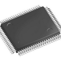
SAF-XC164CS-16F40F BB Infineon Technologies, SAF-XC164CS-16F40F BB Datasheet - Page 47

SAF-XC164CS-16F40F BB
Manufacturer Part Number
SAF-XC164CS-16F40F BB
Description
IC MCU 16BIT FLASH TQFP-100-16
Manufacturer
Infineon Technologies
Series
XC16xr
Datasheet
1.SAF-XC164CS-16F20F_BB.pdf
(80 pages)
Specifications of SAF-XC164CS-16F40F BB
Core Processor
C166SV2
Core Size
16-Bit
Speed
40MHz
Connectivity
CAN, EBI/EMI, SPI, UART/USART
Peripherals
PWM, WDT
Number Of I /o
79
Program Memory Size
128KB (128K x 8)
Program Memory Type
FLASH
Ram Size
8K x 8
Voltage - Supply (vcc/vdd)
2.35 V ~ 2.7 V
Data Converters
A/D 14x8/10b
Oscillator Type
Internal
Operating Temperature
-40°C ~ 85°C
Package / Case
100-LFQFP
Data Bus Width
16 bit
Data Ram Size
8 KB
Interface Type
2xASC, 2xSSC
Maximum Clock Frequency
40 MHz
Number Of Programmable I/os
79
Number Of Timers
11
Operating Supply Voltage
5 V
Maximum Operating Temperature
+ 85 C
Mounting Style
SMD/SMT
Minimum Operating Temperature
- 40 C
On-chip Adc
10 bit, 14 Channel
Packages
PG-TQFP-100
Max Clock Frequency
40.0 MHz
Sram (incl. Cache)
8.0 KByte
Can Nodes
2
A / D Input Lines (incl. Fadc)
14
Program Memory
128.0 KByte
For Use With
B158-H8962-X-X-7600IN - KIT EASY XC164CSMCBX167-NET - BOARD EVAL INFINEON CAN/ETHRNTMCBXC167-BASIC - BOARD EVAL BASIC INFINEON XC16X
Lead Free Status / RoHS Status
Lead free / RoHS Compliant
Eeprom Size
-
Lead Free Status / Rohs Status
Details
Other names
FX164CS16F40FBBNP
FX164CS16F40FBBXT
SAFXC164CS16F40FBBT
SP000094312
SP000224552
FX164CS16F40FBBXT
SAFXC164CS16F40FBBT
SP000094312
SP000224552
3.15
The Clock Generation Unit uses a programmable on-chip PLL with multiple prescalers
to generate the clock signals for the XC164CS with high flexibility. The master clock
is the reference clock signal, and is used for TwinCAN and is output to the external
system. The CPU clock
either directly (1:1) or via a 2:1 prescaler (
The on-chip oscillator can drive an external crystal or accepts an external clock signal.
The oscillator clock frequency can be multiplied by the on-chip PLL (by a programmable
factor) or can be divided by a programmable prescaler factor.
If the bypass mode is used (direct drive or prescaler) the PLL can deliver an independent
clock to monitor the clock signal generated by the on-chip oscillator. This PLL clock is
independent from the XTAL1 clock. When the expected oscillator clock transitions are
missing the Oscillator Watchdog (OWD) activates the PLL Unlock/OWD interrupt node
and supplies the CPU with an emergency clock, the PLL clock signal. Under these
circumstances the PLL will oscillate with its basic frequency.
The oscillator watchdog can be disabled by switching the PLL off. This reduces power
consumption, but also no interrupt request will be generated in case of a missing
oscillator clock.
Note: At the end of an external reset (EA = ‘0’) the oscillator watchdog may be disabled
3.16
The XC164CS provides up to 79 I/O lines which are organized into six input/output ports
and one input port. All port lines are bit-addressable, and all input/output lines are
individually (bit-wise) programmable as inputs or outputs via direction registers. The I/O
ports are true bidirectional ports which are switched to high impedance state when
configured as inputs. The output drivers of some I/O ports can be configured (pin by pin)
for push/pull operation or open-drain operation via control registers. During the internal
reset, all port pins are configured as inputs (except for pin RSTOUT).
The edge characteristics (shape) and driver characteristics (output current) of the port
drivers can be selected via registers POCONx.
The input threshold of some ports is selectable (TTL or CMOS like), where the special
CMOS like input threshold reduces noise sensitivity due to the input hysteresis. The
input threshold may be selected individually for each byte of the respective ports.
All port lines have programmable alternate input or output functions associated with
them. All port lines that are not used for these alternate functions may be used as general
purpose IO lines.
Data Sheet
via hardware by (externally) pulling the RD line low upon a reset, similar to the
standard reset configuration.
Clock Generation
Parallel Ports
f
CPU
and the system clock
f
45
SYS
=
f
CPU
f
SYS
=
are derived from the master clock
f
MC
/ 2). See also
Functional Description
Section
Derivatives
V2.3, 2006-08
XC164CS
4.4.1.
f
MC


