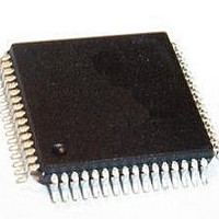
SAK-XC164CM-8F20F AA Infineon Technologies, SAK-XC164CM-8F20F AA Datasheet - Page 21

SAK-XC164CM-8F20F AA
Manufacturer Part Number
SAK-XC164CM-8F20F AA
Description
IC MCU 16BIT 64KB FLSH TQFP-64-8
Manufacturer
Infineon Technologies
Series
XC16xr
Datasheet
1.SAF-XC164CM-4F20F_AA.pdf
(70 pages)
Specifications of SAK-XC164CM-8F20F AA
Core Processor
C166SV2
Core Size
16-Bit
Speed
20MHz
Connectivity
CAN, SPI, UART/USART
Peripherals
PWM, WDT
Number Of I /o
47
Program Memory Size
64KB (64K x 8)
Program Memory Type
FLASH
Ram Size
6K x 8
Voltage - Supply (vcc/vdd)
2.35 V ~ 2.7 V
Data Converters
A/D 14x8/10b
Oscillator Type
Internal
Operating Temperature
-40°C ~ 125°C
Package / Case
64-LFQFP
Data Bus Width
16 bit
Data Ram Size
6 KB
Interface Type
2xASC, 2xSSC
Maximum Clock Frequency
20 MHz
Number Of Programmable I/os
47
Number Of Timers
9
Operating Supply Voltage
5 V
Maximum Operating Temperature
+ 125 C
Mounting Style
SMD/SMT
Minimum Operating Temperature
- 40 C
On-chip Adc
10 bit, 14 Channel
Packages
PG-LQFP-64
Max Clock Frequency
20.0 MHz
Sram (incl. Cache)
6.0 KByte
Can Nodes
2
A / D Input Lines (incl. Fadc)
14
Program Memory
64.0 KByte
For Use With
B158-H8961-X-X-7600IN - KIT EASY XC164CMXC164CMUCANIN - KIT U-CAN STARTER XC164CMMCBX167-NET - BOARD EVAL INFINEON CAN/ETHRNTMCBXC167-BASIC - BOARD EVAL BASIC INFINEON XC16X
Lead Free Status / RoHS Status
Lead free / RoHS Compliant
Eeprom Size
-
Lead Free Status / Rohs Status
Details
Other names
SAK-XC164CM-8F20FAACT
SAK-XC164CM-8F20FAACT
SAK-XC164CM-8F20FAAINCT
SAK-XC164CM-8F20FAACT
SAK-XC164CM-8F20FAAINCT
example, shift and rotate instructions are always processed during one machine cycle
independent of the number of bits to be shifted. Also multiplication and most MAC
instructions execute in one single cycle. All multiple-cycle instructions have been
optimized so that they can be executed very fast as well: for example, a 32-/16-bit
division is started within 4 cycles, while the remaining 15 cycles are executed in the
background. Another pipeline optimization, the branch target prediction, allows
eliminating the execution time of branch instructions if the prediction was correct.
The CPU has a register context consisting of up to three register banks with 16 word
wide GPRs each at its disposal. One of these register banks is physically allocated within
the on-chip DPRAM area. A Context Pointer (CP) register determines the base address
of the active register bank to be accessed by the CPU at any time. The number of
register banks is only restricted by the available internal RAM space. For easy parameter
passing, a register bank may overlap others.
A system stack of up to 32 Kwords is provided as a storage for temporary data. The
system stack can be allocated to any location within the address space (preferably in the
on-chip RAM area), and it is accessed by the CPU via the stack pointer (SP) register.
Two separate SFRs, STKOV and STKUN, are implicitly compared against the stack
pointer value upon each stack access for the detection of a stack overflow or underflow.
The high performance offered by the hardware implementation of the CPU can efficiently
be utilized by a programmer via the highly efficient XC164CM instruction set which
includes the following instruction classes:
•
•
•
•
•
•
•
•
•
•
•
•
•
The basic instruction length is either 2 or 4 bytes. Possible operand types are bits, bytes
and words. A variety of direct, indirect or immediate addressing modes are provided to
specify the required operands.
Data Sheet
Standard Arithmetic Instructions
DSP-Oriented Arithmetic Instructions
Logical Instructions
Boolean Bit Manipulation Instructions
Compare and Loop Control Instructions
Shift and Rotate Instructions
Prioritize Instruction
Data Movement Instructions
System Stack Instructions
Jump and Call Instructions
Return Instructions
System Control Instructions
Miscellaneous Instructions
19
Functional Description
Derivatives
V1.4, 2007-03
XC164CM


