SAK-C164CM-4EF AB Infineon Technologies, SAK-C164CM-4EF AB Datasheet
SAK-C164CM-4EF AB
Specifications of SAK-C164CM-4EF AB
SAK-C164CM-4EFABINTR
SAK-C164CM-4EFABTR
SAK-C164CM-4EFABTR
SAKC164CM4EFABXT
SP000056829
SP000104063


Related parts for SAK-C164CM-4EF AB


SAK-C164CM-4EF AB Summary of contents
Page 1
cro c on tro cro ...
Page 2
... Infineon Technologies Office. Infineon Technologies Components may only be used in life-support devices or systems with the express written approval of Infineon Technologies failure of such components can reasonably be expected to cause the failure of that life-support device or system affect the safety or effectiveness of that device or system. Life support devices or systems are intended to be implanted in the human body support and/or maintain and sustain and/or protect human life ...
Page 3
cro c on tro cro ...
Page 4
C164CM Revision History: Previous Version: Page Subjects (major changes since last revision) Controller Area Network (CAN): License of Robert Bosch GmbH We Listen to Your Comments Any information within this document that you feel is wrong, unclear or missing at ...
Page 5
Single-Chip Microcontroller C166 Family C164CM, C164SM • High Performance 16-bit CPU with 4-Stage Pipeline – Instruction Cycle Time at 25 MHz CPU Clock – 400 ns Multiplication (16 × 16 bit), 800 ns Division ( ...
Page 6
... SAF-C164CM-4R25F SAK-C164SM-4RF SAF-C164SM-4RF SAK-C164SM-4R25F SAF-C164SM-4R25F SAK-C164CM-4EF SAF-C164CM-4EF 1) This Data Sheet is valid for ROM(less) devices starting with and including design step AA, and for OTP devices starting with and including design step AA. For simplicity all versions are referred to by the term C164CM throughout this document. ...
Page 7
Ordering Information The ordering code for Infineon microcontrollers provides an exact reference to the required product. This ordering code identifies: • the derivative itself, i.e. its function set, the temperature range, and the supply voltage • the package and the ...
Page 8
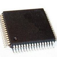
Pin Configuration (top view) 64 P5.3/AN3/T3IN 1 P5.4/AN4/T2EUD 2 P5.5/AN5/T4EUD 3 P5.6/AN6/T2IN 4 P5.7/AN7/T4IN (TRSEL P0.15/AD15/SCLK 8 P0.14/AD14/MTSR 9 P0.13/AD13/MRST 10 P0.12/AD12/RxD0 11 P0.11/AD11/TxD0 12 P0.10/AD10 13 P0.9/AD9 14 P0.8/AD8 ...
Page 9
Table 2 Pin Definitions and Functions Symbol Pin Input No. Outp. PORT0 IO P0H.7 8 (I)/O I/O P0H.6 9 (I)/O I/O P0H.5 10 (I)/O I/O P0H.4 11 (I)/O I/O P0H.3 12 (I)/O O P0H.2 13 (I)/O P0H.1 14 (I)/O P0H.0 ...
Page 10
Table 2 Pin Definitions and Functions (cont’d) Symbol Pin Input No. Outp. RSTIN 27 I/O Data Sheet Function Reset Input with Schmitt-Trigger characteristics. A low level at this pin while the oscillator is running resets the C164CM. An internal pullup ...
Page 11
Table 2 Pin Definitions and Functions (cont’d) Symbol Pin Input No. Outp. P20 IO P20 P20 P20 P20 – P20 P20. Data Sheet Function Port 20 is ...
Page 12
Table 2 Pin Definitions and Functions (cont’d) Symbol Pin Input No. Outp. PORT1 IO P1L.0 36 I/O P1L P1L.2 38 I/O P1L P1L.4 40 I/O P1L P1L P1L P1H.0 44 ...
Page 13
Table 2 Pin Definitions and Functions (cont’d) Symbol Pin Input No. Outp P8.0 56 I/O I P8.1 57 I/O O P8.2 58 I/O I P8 P5.2 64 ...
Page 14
Note: The following behavior differences must be observed when the bidirectional reset is active: • Bit BDRSTEN in register SYSCON cannot be changed after EINIT and is cleared automatically after a reset. • The reset indication flags always indicate a ...
Page 15
Functional Description The architecture of the C164CM combines advantages of both RISC and CISC processors and of advanced peripheral subsystems in a very well-balanced way. In addition the on-chip memory blocks allow the design of compact systems with maximum performance. ...
Page 16
Memory Organization The memory space of the C164CM is configured in a Von Neumann architecture which means that code memory, data memory, registers and I/O ports are organized within the same linear address space which includes 16 MBytes. The entire ...
Page 17
External Bus Controller All of the external memory accesses are performed by a particular on-chip External Bus Controller (EBC). It can be programmed either to Single Chip Mode when no external memory is required one of two different ...
Page 18
Central Processing Unit (CPU) The main core of the CPU consists of a 4-stage instruction pipeline, a 16-bit arithmetic and logic unit (ALU) and dedicated SFRs. Additional hardware has been spent for a separate multiply and divide unit, a bit-mask ...
Page 19
The CPU has a register context consisting wordwide GPRs at its disposal. These 16 GPRs are physically allocated within the on-chip RAM area. A Context Pointer (CP) register determines the base address of the active register ...
Page 20
Interrupt System With an interrupt response time within a range from just CPU clocks (in case of internal program execution), the C164CM is capable of reacting very fast to the occurrence of non-deterministic events. The architecture of ...
Page 21
Table 3 C164CM Interrupt Nodes Source of Interrupt or PEC Service Request Fast External Interrupt 0 CC8IR Fast External Interrupt 1 CC9IR Fast External Interrupt 2 CC10IR Fast External Interrupt 3 CC11IR GPT1 Timer 2 GPT1 Timer 3 GPT1 Timer ...
Page 22
Table 3 C164CM Interrupt Nodes (cont’d) Source of Interrupt or PEC Service Request CAPCOM 6 Timer 12 CAPCOM 6 Timer 13 CAPCOM 6 Emergency Data Sheet Request Enable Flag Flag T12IR T12IE T13IR T13IE CC6EIR CC6EIE 18 Interrupt Vector Vector ...
Page 23
The C164CM also provides an excellent mechanism to identify and to process exceptions or error conditions that arise during run-time, so-called ‘Hardware Traps’. Hardware traps cause immediate non-maskable system reaction which is similar to a standard interrupt service (branching to ...
Page 24
The Capture/Compare Unit CAPCOM2 The general purpose CAPCOM2 unit supports generation and control of timing sequences channels with a maximum resolution of 16 TCL. The CAPCOM units are typically used to handle high speed I/O tasks ...
Page 25
The Capture/Compare Unit CAPCOM6 The CAPCOM6 unit supports generation and control of timing sequences three 16-bit capture/compare channels plus one 10-bit compare channel. In compare mode the CAPCOM6 unit provides two output signals per channel which have ...
Page 26
General Purpose Timer (GPT) Unit The GPT unit represents a very flexible multifunctional timer/counter structure which may be used for many different time related tasks such as event timing and counting, pulse width and duty cycle measurements, pulse generation, or ...
Page 27
T2EUD CPU T2IN CPU T3IN T3EUD T4IN CPU T4EUD … 10 Figure 6 Block Diagram of GPT1 Data Sheet U/D GPT1 Timer ...
Page 28
Real Time Clock The Real Time Clock (RTC) module of the C164CM consists of a chain of 3 divider blocks, a fixed 8:1 divider, the reloadable 16-bit timer T14, and the 32-bit RTC timer (accessible via registers RTCH and RTCL). ...
Page 29
A/D Converter For analog signal measurement, a 10-bit A/D converter with 8 multiplexed input channels and a sample and hold circuit has been integrated on-chip. It uses the method of successive approximation. The sample time (for loading the capacitors) and ...
Page 30
Serial Channels Serial communication with other microcontrollers, processors, terminals or external peripheral components is provided by two serial interfaces with different functionality, an Asynchronous/Synchronous Serial Channel (ASC0) and a High-Speed Synchronous Serial Channel (SSC). The ASC0 is upward compatible with ...
Page 31
CAN-Module The integrated CAN-Module handles the completely autonomous transmission and reception of CAN frames in accordance with the CAN specification V2.0 part B (active), i.e. the on-chip CAN-Modules can receive and transmit standard frames with 11-bit identifiers as well as ...
Page 32
Parallel Ports The C164CM provides I/O lines which are organized into four input/output ports and one input port. All port lines are bit-addressable, and all input/output lines are individually (bit-wise) programmable as inputs or outputs via direction ...
Page 33
Oscillator Watchdog The Oscillator Watchdog (OWD) monitors the clock signal generated by the on-chip oscillator (either with a crystal or via external clock drive). For this operation the PLL provides a clock signal which is used to supervise transitions on ...
Page 34
Power Management The C164CM provides several means to control the power it consumes either at a given time or averaged over a certain timespan. Three mechanisms can be used (partly in parallel): • Power Saving Modes switch the C164CM into ...
Page 35
Instruction Set Summary Table 6 lists the instructions of the C164CM in a condensed way. The various addressing modes that can be used with a specific instruction, the operation of the instructions, parameters for conditional execution of instructions, and the ...
Page 36
Table 6 Instruction Set Summary (cont’d) Mnemonic Description MOV(B) Move word (byte) data MOVBS Move byte operand to word operand with sign extension MOVBZ Move byte operand to word operand with zero extension JMPA, JMPI, Jump absolute/indirect/relative if condition is ...
Page 37
Special Function Registers Overview Table 7 lists all SFRs which are implemented in the C164CM in alphabetical order. Bit-addressable SFRs are marked with the letter “b” in column “Name”. SFRs within the Extended SFR-Space (ESFRs) are marked with the letter ...
Page 38
Table 7 C164CM Registers, Ordered by Name (cont’d) Name Physical Address C1MCFGn EFn6 H C1MCRn EFn0 H C1PCIR EF02 H C1UARn EFn2 H C1UGML EF08 H C1UMLM EF0C H CC16 FE60 H CC16IC b F160 H CC17 FE62 H CC17IC ...
Page 39
Table 7 C164CM Registers, Ordered by Name (cont’d) Name Physical Address CC27IC b F176 H CC28 FE78 H CC28IC b F178 CC29 FE7A H CC29IC b F184 CC30 FE7C H CC30IC b F18C E ...
Page 40
Table 7 C164CM Registers, Ordered by Name (cont’d) Name Physical Address DP0L b F100 H DP1H b F106 H DP1L b F104 H DP20 b FFB6 H DP8 b FFD6 H DPP0 FE00 H DPP1 FE02 H DPP2 FE04 H ...
Page 41
Table 7 C164CM Registers, Ordered by Name (cont’d) Name Physical Address P5 b FFA2 H P5DIDIS b FFA4 H P20 b FFB4 FFD4 H PECC0 FEC0 H PECC1 FEC2 H PECC2 FEC4 H PECC3 FEC6 H PECC4 ...
Page 42
Table 7 C164CM Registers, Ordered by Name (cont’d) Name Physical Address S0RIC b FF6E H S0TBIC b F19C H S0TBUF FEB0 H S0TIC b FF6C H SP FE12 H SSCBR F0B4 H SSCCON b FFB2 H SSCEIC b FF76 H ...
Page 43
Table 7 C164CM Registers, Ordered by Name (cont’d) Name Physical Address T2IC b FF60 H T3 FE42 H T3CON b FF42 H T3IC b FF62 H T4 FE44 H T4CON b FF44 H T4IC b FF64 H T7 F050 H ...
Page 44
Absolute Maximum Ratings Table 8 Absolute Maximum Rating Parameters Parameter Storage temperature Junction temperature V Voltage on pins with DD V respect to ground ( ) SS Voltage on any pin with V respect to ground ( ) SS Input ...
Page 45
... > < C164CM C164SM Unit Notes V Active mode MHz CPUmax V PowerDown mode V Reference voltage 2)3) mA Per pin Pin drivers in default mode °C SAB-C164CM … °C SAF-C164CM … °C SAK-C164CM … - 0.5 V). The absolute sum of input overload V1.0, 2001-05 4) ...
Page 46
Parameter Interpretation The parameters listed in the following partly represent the characteristics of the C164CM and partly its demands on the system. To aid in interpreting the parameters right, when evaluating them for a design, they are marked in column ...
Page 47
DC Characteristics (cont’d) (Operating Conditions apply) Parameter 9) ALE inactive current 9) ALE active current PORT0 configuration current XTAL1 input current 11) Pin capacitance (digital inputs/outputs) 1) Keeping signal levels within the levels specified in this table, ensures operation without ...
Page 48
Power Consumption C164CM (ROM) (Operating Conditions apply) Parameter Power supply current (active) with all peripherals active Idle mode supply current with all peripherals active Idle mode supply current with all peripherals deactivated, PLL off, SDD factor = 32 Sleep and ...
Page 49
Power Consumption C164CM (OTP) (cont’d) (Operating Conditions apply) Parameter Sleep and Power-down mode supply current with RTC running Sleep and Power-down mode supply current with RTC disabled 1) The supply current is a function of the operating frequency. This dependency ...
Page 50
I [mA] 100 Figure 9 Supply/Idle Current as a Function of Operating Frequency for ROM Derivatives Data Sheet C164CM C164SM I DD5max I DD5typ I IDX5max I IDX5typ 25 f [MHz] CPU ...
Page 51
I [mA] 100 Figure 10 Supply/Idle Current as a Function of Operating Frequency for OTP Derivatives Data Sheet C164CM C164SM I DD5max I DD5typ I IDX5max I IDX5typ 25 f [MHz] CPU ...
Page 52
AC Characteristics Definition of Internal Timing The internal operation of the C164CM is controlled by the internal CPU clock edges of the CPU clock can trigger internal (e.g. pipeline) or external (e.g. bus cycles) operations. The specification of the external ...
Page 53
P0.15-13 (P0H.7-5). Register RP0H can be loaded from the upper half of register RSTCON under software control. Table 11 associates the combinations of these three bits with the respective clock generation mode. Table 11 C164CM Clock Generation Modes 1) CLKCFG ...
Page 54
Due to this adaptation to the input clock the frequency locked to . The slight variation causes a jitter of OSC duration of individual TCLs. The timings listed in the AC Characteristics that refer to TCLs ...
Page 55
Direct Drive When direct drive is configured (CLKCFG = 011 disabled and the CPU clock is directly driven from the internal oscillator with the input clock signal. f The frequency of directly follows the frequency of CPU f (i.e. the ...
Page 56
AC Characteristics External Clock Drive XTAL1 (Operating Conditions apply) Table 12 External Clock Drive Characteristics Parameter Symbol t Oscillator period SR 40 OSC 2) t High time Low time Rise ...
Page 57
A/D Converter Characteristics (Operating Conditions apply) Table 13 A/D Converter Characteristics Parameter Analog reference supply Analog reference ground Analog input voltage range Basic clock frequency Conversion time Calibration time after reset Total unadjusted error Internal resistance of reference voltage source ...
Page 58
During the sample time the input capacitance internal resistance of the analog source must allow the capacitance to reach its final voltage level within After the end of the sample time t Values for the sample time S Sample ...
Page 59
Testing Waveforms 2 inputs during testing are driven at 2.4 V for a logic ’1’ and 0.45 V for a logic ’0’. Timing measurements are made at Figure 14 Input Output Waveforms V + 0.1 V ...
Page 60
Memory Cycle Variables The timing tables below use three variables which are derived from the BUSCONx registers and represent the special characteristics of the programmed memory cycle. The following table describes, how these variables are to be computed. Table 15 ...
Page 61
Multiplexed Bus (cont’d) (Operating Conditions apply) ALE cycle time = 6 TCL + 2 Parameter RD, WR low time (no RW-delay valid data in (with RW-delay valid data in (no RW-delay) ALE low to valid data ...
Page 62
ALE (A10-A8) t Read Cycle BUS RD Write Cycle BUS WR Figure 16 External Memory Cycle: Multiplexed Bus, With Read/Write Delay, Normal ALE Data Sheet Address Address ...
Page 63
ALE (A10-A8 Read Cycle BUS RD Write Cycle BUS WR Figure 17 External Memory Cycle: Multiplexed Bus, With Read/Write Delay, Extended ALE Data Sheet Address t 7 Address ...
Page 64
ALE (A10-A8) t Read Cycle BUS RD Write Cycle BUS WR Figure 18 External Memory Cycle: Multiplexed Bus, No Read/Write Delay, Normal ALE Data Sheet Address Address ...
Page 65
ALE (A10-A8 Read Cycle BUS RD Write Cycle BUS WR Figure 19 External Memory Cycle: Multiplexed Bus, No Read/Write Delay, Extended ALE Data Sheet Address t 7 Address ...
Page 66
AC Characteristics CLKOUT (Operating Conditions apply) Parameter CLKOUT cycle time CLKOUT high time CLKOUT low time CLKOUT rise time CLKOUT fall time CLKOUT rising edge to ALE falling edge CLKOUT ALE Command RD, WR Figure 20 CLKOUT Timing Notes 1) ...
Page 67
Package Outlines P-TQFP-64-4 (Plastic Metric Quad Flat Package) Sorts of Packing Package outlines for tubes, trays etc. are contained in our Data Book “Package Information”. SMD = Surface Mounted Device Data Sheet 63 C164CM C164SM Dimensions in mm V1.0, 2001-05 ...
Page 68
... Better operating results and business excellence mean less idleness and wastefulness for all of us, more professional success, more accurate information, a better overview and, thereby, less frustration and more satisfaction.” Dr. Ulrich Schumacher Published by Infineon Technologies AG ...