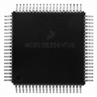
MC9S12E256VFUE Freescale Semiconductor, MC9S12E256VFUE Datasheet - Page 438

MC9S12E256VFUE
Manufacturer Part Number
MC9S12E256VFUE
Description
IC MCU 256K FLASH 25MHZ 80-QFP
Manufacturer
Freescale Semiconductor
Series
HCS12r
Datasheet
1.MC9S12E256CFUE.pdf
(602 pages)
Specifications of MC9S12E256VFUE
Core Processor
HCS12
Core Size
16-Bit
Speed
25MHz
Connectivity
EBI/EMI, I²C, SCI, SPI
Peripherals
POR, PWM, WDT
Number Of I /o
60
Program Memory Size
256KB (256K x 8)
Program Memory Type
FLASH
Ram Size
16K x 8
Voltage - Supply (vcc/vdd)
2.35 V ~ 2.75 V
Data Converters
A/D 16x10b; D/A 2x8b
Oscillator Type
Internal
Operating Temperature
-40°C ~ 105°C
Package / Case
80-QFP
Processor Series
S12E
Core
HCS12
Data Bus Width
16 bit
Data Ram Size
16 KB
Interface Type
I2C, SCI, SPI
Maximum Clock Frequency
50 MHz
Number Of Programmable I/os
60
Number Of Timers
12
Maximum Operating Temperature
+ 105 C
Mounting Style
SMD/SMT
3rd Party Development Tools
EWHCS12
Minimum Operating Temperature
- 40 C
On-chip Adc
10 bit, 16 Channel
On-chip Dac
8 bit, 2 Channel
Package
80PQFP
Family Name
HCS12
Maximum Speed
50 MHz
For Use With
M68EVB912E128 - BOARD EVAL FOR MC9S12E128/64
Lead Free Status / RoHS Status
Lead free / RoHS Compliant
Eeprom Size
-
Lead Free Status / Rohs Status
Details
Available stocks
Company
Part Number
Manufacturer
Quantity
Price
Company:
Part Number:
MC9S12E256VFUE
Manufacturer:
Freescale Semiconductor
Quantity:
10 000
- Current page: 438 of 602
- Download datasheet (4Mb)
Chapter 14 Dual Output Voltage Regulator (VREG3V3V2)
14.1.3
Figure 14-1
consists of two parallel sub-blocks, REG1 and REG2, providing two independent output voltages.
438
V
V
V
DDR
DDA
SSA
Block Diagram
shows the function principle of VREG by means of a block diagram. The regulator core REG
V
REGEN
LVD
Figure 14-1. VREG3V3 Block Diagram
CTRL
MC9S12E256 Data Sheet, Rev. 1.08
REG2
REG1
LVR
REG: Regulator Core
LVD: Low Voltage Detect
CTRL: Regulator Control
LVR: Low Voltage Reset
POR: Power-on Reset
PIN
LVI
LVR
POR
Freescale Semiconductor
POR
V
V
V
V
DDPLL
SSPLL
DD
SS
Related parts for MC9S12E256VFUE
Image
Part Number
Description
Manufacturer
Datasheet
Request
R
Part Number:
Description:
Manufacturer:
Freescale Semiconductor, Inc
Datasheet:
Part Number:
Description:
Manufacturer:
Freescale Semiconductor, Inc
Datasheet:
Part Number:
Description:
Manufacturer:
Freescale Semiconductor, Inc
Datasheet:
Part Number:
Description:
Manufacturer:
Freescale Semiconductor, Inc
Datasheet:
Part Number:
Description:
Manufacturer:
Freescale Semiconductor, Inc
Datasheet:
Part Number:
Description:
Manufacturer:
Freescale Semiconductor, Inc
Datasheet:
Part Number:
Description:
Manufacturer:
Freescale Semiconductor, Inc
Datasheet:
Part Number:
Description:
Manufacturer:
Freescale Semiconductor, Inc
Datasheet:
Part Number:
Description:
Manufacturer:
Freescale Semiconductor, Inc
Datasheet:
Part Number:
Description:
Manufacturer:
Freescale Semiconductor, Inc
Datasheet:
Part Number:
Description:
Manufacturer:
Freescale Semiconductor, Inc
Datasheet:
Part Number:
Description:
Manufacturer:
Freescale Semiconductor, Inc
Datasheet:
Part Number:
Description:
Manufacturer:
Freescale Semiconductor, Inc
Datasheet:
Part Number:
Description:
Manufacturer:
Freescale Semiconductor, Inc
Datasheet:
Part Number:
Description:
Manufacturer:
Freescale Semiconductor, Inc
Datasheet:


