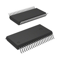
M30263F6AFP#U3 Renesas Electronics America, M30263F6AFP#U3 Datasheet - Page 266

M30263F6AFP#U3
Manufacturer Part Number
M30263F6AFP#U3
Description
MCU 3/5V 48K I TEMP PB-FREE 42-S
Manufacturer
Renesas Electronics America
Series
M16C™ M16C/Tiny/26r
Datasheet
1.M30260F3AGPU5A.pdf
(354 pages)
Specifications of M30263F6AFP#U3
Core Processor
M16C/60
Core Size
16-Bit
Speed
20MHz
Connectivity
I²C, IEBus, SIO, UART/USART
Peripherals
DMA, PWM, Voltage Detect, WDT
Number Of I /o
33
Program Memory Size
48KB (48K x 8)
Program Memory Type
FLASH
Ram Size
2K x 8
Voltage - Supply (vcc/vdd)
2.7 V ~ 5.5 V
Data Converters
A/D 10x10b
Oscillator Type
Internal
Operating Temperature
-40°C ~ 85°C
Package / Case
42-SSOP
Lead Free Status / RoHS Status
Lead free / RoHS Compliant
Eeprom Size
-
- Current page: 266 of 354
- Download datasheet (4Mb)
R
R
M
17.7 Software Commands
e
E
1
. v
J
6
Table 17.7.1. Software Commands
SRD: Status register data (D
WA : Write address (However,even address)
WD : Write data (16 bits)
BA : Highest-order block address (However,even address)
xx : 8 high-order bits of command code (ignored)
0
X : Any even address in the user ROM area
C
17.7.1 Read Array Command (FF
17.7.2 Read Status Register Command (70
2
Read array
9
Read status register
Clear status register
Block erase
Program
0 .
B
2 /
Read or write 16-bit commands and data from or to even addresses in the user ROM area. When writing
a command code, 8 high-order bits (D
0
0
6
2
A
0
This command reads the flash memory.
By writing command code ‘xxFF
specified address can be read in 16-bit unit after the next bus cycle. The microcomputer remains in
read array mode until an another command is written. Therefore, contents of multiple addresses can
be read consecutively.
This command reads the status register.
By writing command code ‘xx70
bus cycle (Refer to 17.8 Status Register). Read an even address in the user ROM area. Do not
execute this command in EW1 mode.
F
2
e
G
0 -
b
Command
o r
1 .
2
0
, 5
u
0
p
2
(
0
M
0
7
1
6
C
page 247
2 /
6
, A
M
7
to D
1
f o
6
C
3
Mode
Write
Write
Write
Write
Write
0
2
2 /
)
9
6
, B
16
16
M
’ in the first bus cycle, the status register can be read in the second
15
’ in the first bus cycle, read array mode is entered. Content of a
First bus cycle
1
6
16
–D
C
Address
)
2 /
8
WA
) are ignored.
6
X
X
X
X
) T
16
(D
xxFF
)
xx70
xx50
xx40
xx20
15
Data
to D
16
16
16
16
16
0
)
Mode
Write
Write
Read
Second bus cycle
Address
17. Flash Memory Version
WA
BA
X
(D
xxD0
15
SRD
Data
WD
to D
16
0
)
Related parts for M30263F6AFP#U3
Image
Part Number
Description
Manufacturer
Datasheet
Request
R

Part Number:
Description:
KIT STARTER FOR M16C/29
Manufacturer:
Renesas Electronics America
Datasheet:

Part Number:
Description:
KIT STARTER FOR R8C/2D
Manufacturer:
Renesas Electronics America
Datasheet:

Part Number:
Description:
R0K33062P STARTER KIT
Manufacturer:
Renesas Electronics America
Datasheet:

Part Number:
Description:
KIT STARTER FOR R8C/23 E8A
Manufacturer:
Renesas Electronics America
Datasheet:

Part Number:
Description:
KIT STARTER FOR R8C/25
Manufacturer:
Renesas Electronics America
Datasheet:

Part Number:
Description:
KIT STARTER H8S2456 SHARPE DSPLY
Manufacturer:
Renesas Electronics America
Datasheet:

Part Number:
Description:
KIT STARTER FOR R8C38C
Manufacturer:
Renesas Electronics America
Datasheet:

Part Number:
Description:
KIT STARTER FOR R8C35C
Manufacturer:
Renesas Electronics America
Datasheet:

Part Number:
Description:
KIT STARTER FOR R8CL3AC+LCD APPS
Manufacturer:
Renesas Electronics America
Datasheet:

Part Number:
Description:
KIT STARTER FOR RX610
Manufacturer:
Renesas Electronics America
Datasheet:

Part Number:
Description:
KIT STARTER FOR R32C/118
Manufacturer:
Renesas Electronics America
Datasheet:

Part Number:
Description:
KIT DEV RSK-R8C/26-29
Manufacturer:
Renesas Electronics America
Datasheet:

Part Number:
Description:
KIT STARTER FOR SH7124
Manufacturer:
Renesas Electronics America
Datasheet:

Part Number:
Description:
KIT STARTER FOR H8SX/1622
Manufacturer:
Renesas Electronics America
Datasheet:

Part Number:
Description:
KIT DEV FOR SH7203
Manufacturer:
Renesas Electronics America
Datasheet:


