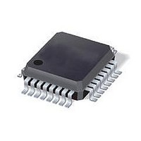
C8051F352 Silicon Laboratories Inc, C8051F352 Datasheet - Page 25

C8051F352
Manufacturer Part Number
C8051F352
Description
IC 8051 MCU 8K FLASH 32LQFP
Manufacturer
Silicon Laboratories Inc
Series
C8051F35xr
Specifications of C8051F352
Core Processor
8051
Core Size
8-Bit
Speed
50MHz
Connectivity
SMBus (2-Wire/I²C), SPI, UART/USART
Peripherals
POR, PWM, Temp Sensor, WDT
Number Of I /o
17
Program Memory Size
8KB (8K x 8)
Program Memory Type
FLASH
Ram Size
768 x 8
Voltage - Supply (vcc/vdd)
2.7 V ~ 3.6 V
Data Converters
A/D 8x16b; D/A 2x8b
Oscillator Type
Internal
Operating Temperature
-40°C ~ 85°C
Package / Case
32-LQFP
Processor Series
C8051F35x
Core
8051
Data Bus Width
8 bit
Data Ram Size
768 B
Interface Type
I2C, SPI, UART
Maximum Clock Frequency
50 MHz
Number Of Programmable I/os
17
Number Of Timers
4
Operating Supply Voltage
2.7 V to 3.6 V
Maximum Operating Temperature
+ 85 C
Mounting Style
SMD/SMT
Minimum Operating Temperature
- 40 C
On-chip Adc
16 bit
On-chip Dac
8 bit
Lead Free Status / RoHS Status
Contains lead / RoHS non-compliant
Eeprom Size
-
Lead Free Status / Rohs Status
No
Available stocks
Company
Part Number
Manufacturer
Quantity
Price
Company:
Part Number:
C8051F352
Manufacturer:
SILICON
Quantity:
364
Company:
Part Number:
C8051F352
Manufacturer:
Silicon Laboratories Inc
Quantity:
10 000
Company:
Part Number:
C8051F352-GQ
Manufacturer:
SiliconL
Quantity:
3 843
Company:
Part Number:
C8051F352-GQ
Manufacturer:
SILICON
Quantity:
4
Company:
Part Number:
C8051F352-GQ
Manufacturer:
Silicon Laboratories Inc
Quantity:
10 000
Part Number:
C8051F352-GQ
Manufacturer:
SILICON LABS/芯科
Quantity:
20 000
Company:
Part Number:
C8051F352-GQR
Manufacturer:
Silicon Laboratories Inc
Quantity:
10 000
Company:
Part Number:
C8051F352-GQR..
Manufacturer:
SILICON
Quantity:
15 000
Company:
Part Number:
C8051F352R
Manufacturer:
Silicon Laboratories Inc
Quantity:
10 000
1.8.
C8051F350/1/2/3 devices include 17 I/O pins. Port pins are organized as two byte-wide ports and one 1-bit
port. The port pins behave like typical 8051 ports with a few enhancements. Each port pin can be config-
ured as a digital or analog I/O pin. Pins selected as digital I/O can be configured for push-pull or open-drain
operation. The “weak pull-ups” that are fixed on typical 8051 devices may be globally disabled to save
power.
The Digital Crossbar allows mapping of internal digital system resources to port I/O pins. On-chip
conter/timers, serial buses, hardware interrupts, and other digital signals can be configured to appear on
the port pins using the Crossbar control resgiters. This allows the user to select the exact mix of general-
purpose port I/O, digital, and analog resources needed for the application.
Highest
Lowest
Priority
Priority
Port Input/Output
SYSCLK
Outputs
SMBus
T0, T1
UART
P0
P1
P2
PCA
CP0
SPI
(P0.0-P0.7)
(P1.0-P1.7)
Figure 1.10. Port I/O Functional Block Diagram
2
2
4
2
4
2
8
8
(P2.0)
PnSKIP Registers
XBR0, XBR1,
Crossbar
Rev. 0.4
Decoder
Priority
Digital
8
8
PnMDIN Registers
PnMDOUT,
C8051F350/1/2/3
Cells
Cells
Cell
I/O
I/O
I/O
P0
P1
P2
P0.0
P0.7
P1.0
P1.7
P2.0
25


