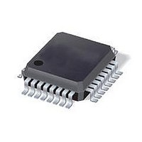
C8051F350 Silicon Laboratories Inc, C8051F350 Datasheet - Page 223

C8051F350
Manufacturer Part Number
C8051F350
Description
IC 8051 MCU 8K FLASH 32LQFP
Manufacturer
Silicon Laboratories Inc
Series
C8051F35xr
Specifications of C8051F350
Core Processor
8051
Core Size
8-Bit
Speed
50MHz
Connectivity
SMBus (2-Wire/I²C), SPI, UART/USART
Peripherals
POR, PWM, Temp Sensor, WDT
Number Of I /o
17
Program Memory Size
8KB (8K x 8)
Program Memory Type
FLASH
Ram Size
768 x 8
Voltage - Supply (vcc/vdd)
2.7 V ~ 3.6 V
Data Converters
A/D 8x24b; D/A 2x8b
Oscillator Type
Internal
Operating Temperature
-40°C ~ 85°C
Package / Case
32-LQFP
Data Bus Width
8 bit
Data Rom Size
128 B
On-chip Adc
10 bit
Number Of Timers
16 bit
Operating Supply Voltage
2.7 V to 3.6 V
Mounting Style
SMD/SMT
Height
1.4 mm
Length
7 mm
Maximum Operating Temperature
+ 85 C
Minimum Operating Temperature
- 40 C
Width
7 mm
Lead Free Status / RoHS Status
Contains lead / RoHS non-compliant
Eeprom Size
-
Lead Free Status / Rohs Status
No RoHS Version Available
Available stocks
Company
Part Number
Manufacturer
Quantity
Price
Company:
Part Number:
C8051F350
Manufacturer:
Silicon Laboratories Inc
Quantity:
10 000
Part Number:
C8051F350
Manufacturer:
SILICON LABS/芯科
Quantity:
20 000
Company:
Part Number:
C8051F350-GQ
Manufacturer:
SiliconL
Quantity:
3 029
Company:
Part Number:
C8051F350-GQ
Manufacturer:
SILICON
Quantity:
18
Company:
Part Number:
C8051F350-GQ
Manufacturer:
Silicon Laboratories Inc
Quantity:
10 000
Company:
Part Number:
C8051F350-GQR
Manufacturer:
Silicon Laboratories Inc
Quantity:
10 000
Part Number:
C8051F350-GQR
Manufacturer:
SILICON LABS/芯科
Quantity:
20 000
Company:
Part Number:
C8051F350DK
Manufacturer:
SiliconL
Quantity:
8
Company:
Part Number:
C8051F350R
Manufacturer:
Silicon Laboratories Inc
Quantity:
10 000
24.
C8051F350/1/2/3 devices include an on-chip Silicon Labs 2-Wire (C2) debug interface to allow Flash pro-
gramming, boundary scan functions, and in-system debugging with the production part installed in the end
application. The C2 interface uses a clock signal (C2CK) and a bi-directional C2 data signal (C2D) to trans-
fer information between the device and a host system. See the C2 Interface Specification for details on the
C2 protocol.
24.1. C2 Interface Registers
The following describes the C2 registers necessary to perform Flash programming and boundary scan
functions through the C2 interface. All C2 registers are accessed through the C2 interface as described in
the C2 Interface Specification.
Bits7-0:
This read-only register returns the 8-bit device ID: 0x0B (C8051F350/1/2/3).
Bit7
Bit7
C2 Interface
The C2ADD register is accessed via the C2 interface to select the target Data register for
C2 Data Read and Data Write commands.
Address
0xB4
0x00
0x01
0x02
Bit6
Bit6
Figure 24.2. DEVICEID: C2 Device ID Register
Figure 24.1. C2ADD: C2 Address Register
Bit5
Bit5
Selects the Device ID register for Data Read instructions
Selects the Revision ID register for Data Read instructions
Selects the C2 Flash Programming Control register for Data
Read/Write instructions
Selects the C2 Flash Programming Data register for Data
Read/Write instructions
Bit4
Bit4
Rev. 0.4
Bit3
Bit3
Description
Bit2
Bit2
C8051F350/1/2/3
Bit1
Bit1
Bit0
Bit0
00000000
Reset Value
Reset Value
00001011
223


