C8051F017 Silicon Laboratories Inc, C8051F017 Datasheet - Page 139
C8051F017
Manufacturer Part Number
C8051F017
Description
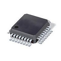
IC 8051 MCU 32K FLASH 32LQFP
Manufacturer
Silicon Laboratories Inc
Series
C8051F01xr
Specifications of C8051F017
Core Processor
8051
Core Size
8-Bit
Speed
25MHz
Connectivity
SMBus (2-Wire/I²C), SPI, UART/USART
Peripherals
Brown-out Detect/Reset, POR, PWM, Temp Sensor, WDT
Number Of I /o
8
Program Memory Size
32KB (32K x 8)
Program Memory Type
FLASH
Ram Size
2.25K x 8
Voltage - Supply (vcc/vdd)
2.7 V ~ 3.6 V
Data Converters
A/D 4x10b; D/A 2x12b
Oscillator Type
Internal
Operating Temperature
-40°C ~ 85°C
Package / Case
32-LQFP
Data Bus Width
8 bit
Data Ram Size
2.25 KB
Interface Type
SMBus, SPI, UART
Maximum Clock Frequency
25 MHz
Number Of Programmable I/os
8
Number Of Timers
16 bit
Operating Supply Voltage
2.7 V to 3.6 V
Maximum Operating Temperature
+ 85 C
Mounting Style
SMD/SMT
Minimum Operating Temperature
- 40 C
On-chip Adc
10 bit, 4 Channel
On-chip Dac
12 bit, 2 Channel
Lead Free Status / RoHS Status
Contains lead / RoHS non-compliant
Eeprom Size
-
Lead Free Status / Rohs Status
No
Available stocks
Company
Part Number
Manufacturer
Quantity
Price
Company:

Part Number:
C8051F017
Manufacturer:
Silicon Laboratories Inc
Quantity:
10 000
Company:
Part Number:
C8051F017-GQ
Manufacturer:
Silicon Labs
Quantity:
135
Company:
Part Number:
C8051F017-GQ
Manufacturer:
Silicon Laboratories Inc
Quantity:
10 000
Company:
Part Number:
C8051F017-GQR
Manufacturer:
Silicon Laboratories Inc
Quantity:
10 000
Company:
Part Number:
C8051F017R
Manufacturer:
Silicon Laboratories Inc
Quantity:
10 000


Setting the TR0 bit (TCON.4) enables the timer when either GATE0 (TMOD.3) is 0 or the input signal /INT0 is
logic-level one. Setting GATE0 to logic 1 allows the timer to be controlled by the external input signal /INT0,
facilitating pulse width measurements.
Setting TR0 does not reset the timer register. The timer register should be initialized to the desired value before
enabling the timer.
TL1 and TH1 form the 13-bit register for Timer 1 in the same manner as described above for TL0 and TH0. Timer
1 is configured and controlled using the relevant TCON and TMOD bits just as with Timer 0.
19.1.2. Mode 1: 16-bit Counter/Timer
Mode 1 operation is the same as Mode 0, except that the counter/timer registers use all 16 bits. The counter/timers
are enabled and configured in Mode 1 in the same manner as for Mode 0.
139
C8051F000/1/2/5/6/7
C8051F010/1/2/5/6/7
SYSCLK
/INT0
T0
GATE0
TR0
Crossbar
Crossbar
12
TR0
0
1
0
1
1
1
X = Don’t Care
Figure 19.1. T0 Mode 0 Block Diagram
CKCON
M
T
2
0
1
M
T
1
GATE0
M
T
0
X
0
1
1
G
A
T
E
1
Rev. 1.7
C
T
/INT0
1
/
M
T
1
1
TMOD
X
X
0
1
M
T
1
0
TCLK
G
A
T
E
0
C
T
0
/
M
T
0
1
M
T
0
0
(5 bits)
Counter/Timer
TL0
Disabled
Disabled
Enabled
Enabled
(8 bits)
TH0
TR1
TR0
TF1
TF0
IE1
IE0
IT1
IT0
Interrupt
Related parts for C8051F017
Image
Part Number
Description
Manufacturer
Datasheet
Request
R

Part Number:
Description:
SMD/C°/SINGLE-ENDED OUTPUT SILICON OSCILLATOR
Manufacturer:
Silicon Laboratories Inc
Part Number:
Description:
Manufacturer:
Silicon Laboratories Inc
Datasheet:
Part Number:
Description:
N/A N/A/SI4010 AES KEYFOB DEMO WITH LCD RX
Manufacturer:
Silicon Laboratories Inc
Datasheet:
Part Number:
Description:
N/A N/A/SI4010 SIMPLIFIED KEY FOB DEMO WITH LED RX
Manufacturer:
Silicon Laboratories Inc
Datasheet:
Part Number:
Description:
N/A/-40 TO 85 OC/EZLINK MODULE; F930/4432 HIGH BAND (REV E/B1)
Manufacturer:
Silicon Laboratories Inc
Part Number:
Description:
EZLink Module; F930/4432 Low Band (rev e/B1)
Manufacturer:
Silicon Laboratories Inc
Part Number:
Description:
I°/4460 10 DBM RADIO TEST CARD 434 MHZ
Manufacturer:
Silicon Laboratories Inc
Part Number:
Description:
I°/4461 14 DBM RADIO TEST CARD 868 MHZ
Manufacturer:
Silicon Laboratories Inc
Part Number:
Description:
I°/4463 20 DBM RFSWITCH RADIO TEST CARD 460 MHZ
Manufacturer:
Silicon Laboratories Inc
Part Number:
Description:
I°/4463 20 DBM RADIO TEST CARD 868 MHZ
Manufacturer:
Silicon Laboratories Inc
Part Number:
Description:
I°/4463 27 DBM RADIO TEST CARD 868 MHZ
Manufacturer:
Silicon Laboratories Inc
Part Number:
Description:
I°/4463 SKYWORKS 30 DBM RADIO TEST CARD 915 MHZ
Manufacturer:
Silicon Laboratories Inc
Part Number:
Description:
N/A N/A/-40 TO 85 OC/4463 RFMD 30 DBM RADIO TEST CARD 915 MHZ
Manufacturer:
Silicon Laboratories Inc
Part Number:
Description:
I°/4463 20 DBM RADIO TEST CARD 169 MHZ
Manufacturer:
Silicon Laboratories Inc