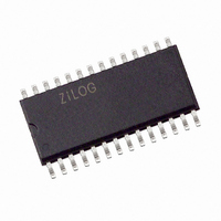
Z8F0812SJ020EC Zilog, Z8F0812SJ020EC Datasheet - Page 151

Z8F0812SJ020EC
Manufacturer Part Number
Z8F0812SJ020EC
Description
IC ENCORE MCU FLASH 8K 28SOIC
Manufacturer
Zilog
Series
Encore!® XP®r
Datasheet
1.Z8F08200100KIT.pdf
(264 pages)
Specifications of Z8F0812SJ020EC
Core Processor
Z8
Core Size
8-Bit
Speed
20MHz
Connectivity
I²C, IrDA, SPI, UART/USART
Peripherals
Brown-out Detect/Reset, POR, PWM, WDT
Number Of I /o
19
Program Memory Size
8KB (8K x 8)
Program Memory Type
FLASH
Ram Size
1K x 8
Voltage - Supply (vcc/vdd)
2.7 V ~ 3.6 V
Oscillator Type
Internal
Operating Temperature
-40°C ~ 105°C
Package / Case
28-SOIC (7.5mm Width)
Lead Free Status / RoHS Status
Contains lead / RoHS non-compliant
Eeprom Size
-
Data Converters
-
Other names
269-3228
- Current page: 151 of 264
- Download datasheet (6Mb)
PS022517-0508
5. After the first bit has been shifted out, a Transmit Interrupt is asserted.
6. Software responds by writing the lower eight bits of address to the I
7. The I
8. If the I
9. The I
10. The I
11. Software responds by setting the START bit of the I
12. Software responds by writing 11110B followed by the 2-bit Slave address and a 1
13. If only one byte is to be read, software sets the NAK bit of the I
14. After the I
15. The I
16. The I
17. The I
18. The I
during the next high period of SCL, the I
Status register. Continue with
If the slave does not acknowledge the first address byte, the I
NCKI bit and clears the ACK bit in the I
Not Acknowledge interrupt by setting the STOP and FLUSH bits and clearing the TXI
bit. The I2C Controller sends the STOP condition on the bus and clears the STOP and
NCKI bits. The transaction is complete (ignore following steps).
Register (second address byte).
I
repeated START and by clearing the TXI bit.
(read) to the I
acknowledge by pulling the SDA signal low during the next high period of SCL, the
I
If the slave does not acknowledge the second address byte, the I
NCKI bit and clears the ACK bit in the I
Not Acknowledge interrupt by setting the STOP and FLUSH bits and clearing the TXI
bit. The I2C Controller sends the STOP condition on the bus and clears the STOP and
NCKI bits. The transaction is complete (ignore the following steps).
Register (third address transfer).
slave read address and a 1 (read).
high period of SCL.
If the slave were to Not Acknowledge at this point (this should not happen because the
slave did acknowledge the first two address bytes), software would respond by setting
the STOP and FLUSH bits and clearing the TXI bit. The I2C Controller sends the
2
2
C Controller generates a Transmit Interrupt.
C Controller sets the ACK bit in the I
2
2
2
2
2
2
2
C Controller completes shifting of the two address bits and a 0 (write).
C Controller loads the I
C Controller shifts out the second address byte. After the first bit is shifted, the
C Controller sends the repeated START condition.
C Controller loads the I
C Controller sends
C Slave sends an acknowledge by pulling the SDA signal Low during the next
2
C Slave acknowledges the first address byte by pulling the SDA signal low
2
C Controller shifts out the 2nd address byte, the I
2
C Data Register.
11110B
2
2
step
C Shift register with the contents of the I
C Shift register with the contents of the I
followed by the two most significant bits of the
9.
2
C Status register. Continue with step 15.
2
2
2
C Status register. Software responds to the
C Status register. Software responds to the
C Controller sets the ACK bit in the I
Z8 Encore! XP
2
C Control Register to generate a
Product Specification
2
2
C Slave sends an
C Controller sets the
2
2
C Controller sets the
C Control Register.
2
®
C Data Register.
F0822 Series
2
2
C Data
C Data
I2C Controller
2
C
138
Related parts for Z8F0812SJ020EC
Image
Part Number
Description
Manufacturer
Datasheet
Request
R

Part Number:
Description:
Communication Controllers, ZILOG INTELLIGENT PERIPHERAL CONTROLLER (ZIP)
Manufacturer:
Zilog, Inc.
Datasheet:

Part Number:
Description:
KIT DEV FOR Z8 ENCORE 16K TO 64K
Manufacturer:
Zilog
Datasheet:

Part Number:
Description:
KIT DEV Z8 ENCORE XP 28-PIN
Manufacturer:
Zilog
Datasheet:

Part Number:
Description:
DEV KIT FOR Z8 ENCORE 8K/4K
Manufacturer:
Zilog
Datasheet:

Part Number:
Description:
KIT DEV Z8 ENCORE XP 28-PIN
Manufacturer:
Zilog
Datasheet:

Part Number:
Description:
DEV KIT FOR Z8 ENCORE 4K TO 8K
Manufacturer:
Zilog
Datasheet:

Part Number:
Description:
CMOS Z8 microcontroller. ROM 16 Kbytes, RAM 256 bytes, speed 16 MHz, 32 lines I/O, 3.0V to 5.5V
Manufacturer:
Zilog, Inc.
Datasheet:

Part Number:
Description:
Low-cost microcontroller. 512 bytes ROM, 61 bytes RAM, 8 MHz
Manufacturer:
Zilog, Inc.
Datasheet:

Part Number:
Description:
Z8 4K OTP Microcontroller
Manufacturer:
Zilog, Inc.
Datasheet:

Part Number:
Description:
CMOS SUPER8 ROMLESS MCU
Manufacturer:
Zilog, Inc.
Datasheet:

Part Number:
Description:
SL1866 CMOSZ8 OTP Microcontroller
Manufacturer:
Zilog, Inc.
Datasheet:

Part Number:
Description:
SL1866 CMOSZ8 OTP Microcontroller
Manufacturer:
Zilog, Inc.
Datasheet:

Part Number:
Description:
OTP (KB) = 1, RAM = 125, Speed = 12, I/O = 14, 8-bit Timers = 2, Comm Interfaces Other Features = Por, LV Protect, Voltage = 4.5-5.5V
Manufacturer:
Zilog, Inc.
Datasheet:

Part Number:
Description:
Manufacturer:
Zilog, Inc.
Datasheet:


