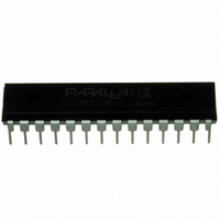
SX28AC/DP-G Parallax Inc, SX28AC/DP-G Datasheet - Page 9

SX28AC/DP-G
Manufacturer Part Number
SX28AC/DP-G
Description
IC MCU 2K FLASH 50MHZ 28DIP
Manufacturer
Parallax Inc
Series
SXr
Datasheet
1.SX20ACSS-G.pdf
(51 pages)
Specifications of SX28AC/DP-G
Core Size
8-Bit
Program Memory Size
3KB (2K x 12)
Oscillator Type
Internal
Core Processor
RISC
Speed
75MHz
Peripherals
Brown-out Detect/Reset, POR, WDT
Number Of I /o
20
Program Memory Type
FLASH
Ram Size
136 x 8
Voltage - Supply (vcc/vdd)
3 V ~ 5.5 V
Operating Temperature
0°C ~ 70°C
Package / Case
28-DIP (0.300", 7.62mm)
Controller Family/series
SX
No. Of I/o's
20
Eeprom Memory Size
2048Byte
Ram Memory Size
136Byte
Cpu Speed
75MHz
Processor Series
Ubicom SXx
Core
RISC
Data Bus Width
8 bit
Data Ram Size
136 B
Maximum Clock Frequency
75 MHz
Number Of Programmable I/os
20
Number Of Timers
1
Operating Supply Voltage
4.5 V to 5.5 V
Maximum Operating Temperature
+ 70 C
Mounting Style
Through Hole
Development Tools By Supplier
32300, 28138, 45302
Minimum Operating Temperature
0 C
Lead Free Status / RoHS Status
Lead free / RoHS Compliant
Eeprom Size
-
Data Converters
-
Connectivity
-
Lead Free Status / Rohs Status
Details
Other names
SX28AC/DP
SX28AC/DP
SX28AC/DP
Parallax SX20AC/SX28AC
3.0
All models contain a 4-bit I/O port (Port A), an 8-bit I/O
port (Port B). The SX28 also contains a second 8-bit I/O
port (Port C). Port A provides symmetrical drive
capability. Each port has three associated 8-bit registers
(Direction, Data, TTL/CMOS Select, and Pull-Up Enable)
to configure each port pin as Hi-Z input or output, to
select TTL or CMOS voltage levels, and to enable/disable
the weak pull-up resistor. The upper four bits of the
3.1.
The three ports are memory-mapped into the data memory
address space. To the CPU, the three ports are available as
the RA, RB, and RC file registers at data memory
addresses 05h, 06h, and 07h, respectively. Writing to a
port data register sets the voltage levels of the
© Parallax Inc.
Output
PORT DESCRIPTIONS
Reading and Writing the Ports
Data Direction Registers:
0
RA, RB, RC
Hi-Z Input
1
Table 3-1: Port Configuration
TTL/CMOS Selected Registers:
CMOS
0
LVL_A, LVL_B, LVL_C
Page 9 of 51
registers associated with Port A are not used. The least
significant bit of the registers corresponds to the least
significant port pin. To access these registers, an
appropriate value must be written into the MODE
register. Upon power-up, all bits in these registers are
initialized to “1”. The associated registers allow for each
port bit to be individually configured under software
controls as shown below.
corresponding port pins that have been configured to
operate as outputs to a corresponding level, 1 = 5 V,
0 = 0 V. Reading from a register reads the voltage levels
of all port pins.
TTL
1
Figure 3-1
Port A Configuration
Enable
0
Pullup Enable Registers:
PLP_A, PLP_B, PLP_C
Rev 1.6 11/20/2006
www.parallax.com
Disable
1


