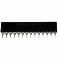
SX28AC/DP-G Parallax Inc, SX28AC/DP-G Datasheet - Page 10

SX28AC/DP-G
Manufacturer Part Number
SX28AC/DP-G
Description
IC MCU 2K FLASH 50MHZ 28DIP
Manufacturer
Parallax Inc
Series
SXr
Datasheet
1.SX20ACSS-G.pdf
(51 pages)
Specifications of SX28AC/DP-G
Core Size
8-Bit
Program Memory Size
3KB (2K x 12)
Oscillator Type
Internal
Core Processor
RISC
Speed
75MHz
Peripherals
Brown-out Detect/Reset, POR, WDT
Number Of I /o
20
Program Memory Type
FLASH
Ram Size
136 x 8
Voltage - Supply (vcc/vdd)
3 V ~ 5.5 V
Operating Temperature
0°C ~ 70°C
Package / Case
28-DIP (0.300", 7.62mm)
Controller Family/series
SX
No. Of I/o's
20
Eeprom Memory Size
2048Byte
Ram Memory Size
136Byte
Cpu Speed
75MHz
Processor Series
Ubicom SXx
Core
RISC
Data Bus Width
8 bit
Data Ram Size
136 B
Maximum Clock Frequency
75 MHz
Number Of Programmable I/os
20
Number Of Timers
1
Operating Supply Voltage
4.5 V to 5.5 V
Maximum Operating Temperature
+ 70 C
Mounting Style
Through Hole
Development Tools By Supplier
32300, 28138, 45302
Minimum Operating Temperature
0 C
Lead Free Status / RoHS Status
Lead free / RoHS Compliant
Eeprom Size
-
Data Converters
-
Connectivity
-
Lead Free Status / Rohs Status
Details
Other names
SX28AC/DP
SX28AC/DP
SX28AC/DP
Parallax SX20AC/SX28AC
For example, suppose all four Port A pins are configured
as outputs and you wish to set RA0 and RA1 high, and
RA2 and RA3 low:
mov W,#$03
mov $05,W
The second “mov” instruction in this example writes the
Port A data register (RA), which controls the output levels
of the four Port A pins, RA0 through RA3. Because Port
A has only four I/O pins, only the four least significant
bits of this register are used. The four high-order register
bits are “don’t care” bits. Port B and Port C are both eight
bits wide, so the full widths of the RB and RC registers
are used.
© Parallax Inc.
;load W with the value 03h
;(bits 0 and 1 high)
;write 03h to Port A data
;register
Page 10 of 51
When a write is performed to a bit position for a port that
has been configured as an input, a write to the port data
register is still performed, but it has no immediate effect
on the pin. If later that pin is configured to operate as an
output, it will reflect the value that has been written to the
data register.
When a read is performed from a bit position for a port,
the operation is actually reading the voltage level on the
pin itself, not necessarily the bit value stored in the port
data register. This is true whether the pin is configured to
operate as an input or an output. Therefore, with the pin
configured to operate as an input, the data register
contents have no effect on the value that you read. With
the pin configured to operate as an output, what is read
generally matches what has been written to the register.
Figure 3-2
Port B, Port C
Configuration
Rev 1.6 11/20/2006
www.parallax.com


