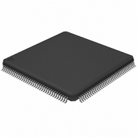
LPC2214FBD144,551 NXP Semiconductors, LPC2214FBD144,551 Datasheet - Page 21

LPC2214FBD144,551
Manufacturer Part Number
LPC2214FBD144,551
Description
IC ARM7 MCU FLASH 256K 144-LQFP
Manufacturer
NXP Semiconductors
Series
LPC2200r
Datasheet
1.LPC2212FBD144015.pdf
(45 pages)
Specifications of LPC2214FBD144,551
Core Processor
ARM7
Core Size
16/32-Bit
Speed
60MHz
Connectivity
EBI/EMI, I²C, Microwire, SPI, SSI, SSP, UART/USART
Peripherals
POR, PWM, WDT
Number Of I /o
112
Program Memory Size
256KB (256K x 8)
Program Memory Type
FLASH
Ram Size
16K x 8
Voltage - Supply (vcc/vdd)
1.65 V ~ 1.95 V
Data Converters
A/D 8x10b
Oscillator Type
Internal
Operating Temperature
-40°C ~ 85°C
Package / Case
144-LQFP
For Use With
OM10091 - KIT DEV PHYCORE-ARM7/LPC2220568-1757 - BOARD EVAL FOR LPC220X ARM MCU
Lead Free Status / RoHS Status
Lead free / RoHS Compliant
Eeprom Size
-
Other names
568-1229
935274741551
LPC2214FBD144-S
935274741551
LPC2214FBD144-S
Available stocks
Company
Part Number
Manufacturer
Quantity
Price
Company:
Part Number:
LPC2214FBD144,551
Manufacturer:
NXP Semiconductors
Quantity:
10 000
NXP Semiconductors
LPC2212_2214_4
Product data sheet
6.17.1 Features
6.17 Pulse width modulator
The PWM is based on the standard Timer block and inherits all of its features, although
only the PWM function is pinned out on the LPC2212/2214. The Timer is designed to
count cycles of the peripheral clock (PCLK) and optionally generate interrupts or perform
other actions when specified timer values occur, based on seven match registers. The
PWM function is also based on match register events.
The ability to separately control rising and falling edge locations allows the PWM to be
used for more applications. For instance, multi-phase motor control typically requires three
non-overlapping PWM outputs with individual control of all three pulse widths and
positions.
Two match registers can be used to provide a single edge controlled PWM output. One
match register (MR0) controls the PWM cycle rate, by resetting the count upon match.
The other match register controls the PWM edge position. Additional single edge
controlled PWM outputs require only one match register each, since the repetition rate is
the same for all PWM outputs. Multiple single edge controlled PWM outputs will all have a
rising edge at the beginning of each PWM cycle, when an MR0 match occurs.
Three match registers can be used to provide a PWM output with both edges controlled.
Again, the MR0 match register controls the PWM cycle rate. The other match registers
control the two PWM edge positions. Additional double edge controlled PWM outputs
require only two match registers each, since the repetition rate is the same for all PWM
outputs.
With double edge controlled PWM outputs, specific match registers control the rising and
falling edge of the output. This allows both positive going PWM pulses (when the rising
edge occurs prior to the falling edge), and negative going PWM pulses (when the falling
edge occurs prior to the rising edge).
•
•
•
•
•
Provides Seconds, Minutes, Hours, Day of Month, Month, Year, Day of Week, and Day
of Year.
Programmable reference clock divider allows adjustment of the RTC to match various
crystal frequencies.
Seven match registers allow up to six single edge controlled or three double edge
controlled PWM outputs, or a mix of both types.
The match registers also allow:
– Continuous operation with optional interrupt generation on match.
– Stop timer on match with optional interrupt generation.
– Reset timer on match with optional interrupt generation.
Supports single edge controlled and/or double edge controlled PWM outputs. Single
edge controlled PWM outputs all go HIGH at the beginning of each cycle unless the
output is a constant LOW. Double edge controlled PWM outputs can have either edge
occur at any position within a cycle. This allows for both positive going and negative
going pulses.
Rev. 04 — 3 January 2008
16/32-bit ARM microcontrollers
LPC2212/2214
© NXP B.V. 2008. All rights reserved.
21 of 45


