AT91SAM7X256-AU-999 Atmel, AT91SAM7X256-AU-999 Datasheet - Page 37
AT91SAM7X256-AU-999
Manufacturer Part Number
AT91SAM7X256-AU-999
Description
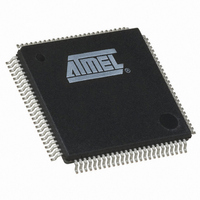
IC ARM7 MCU 256K FLASH 100-LQFP
Manufacturer
Atmel
Series
AT91SAMr
Datasheet
1.AT91SAM7X256B-CU.pdf
(45 pages)
Specifications of AT91SAM7X256-AU-999
Core Processor
ARM7
Core Size
16/32-Bit
Speed
55MHz
Connectivity
CAN, Ethernet, I²C, SPI, SSC, UART/USART, USB
Peripherals
Brown-out Detect/Reset, DMA, POR, PWM, WDT
Number Of I /o
62
Program Memory Size
256KB (256K x 8)
Program Memory Type
FLASH
Ram Size
64K x 8
Voltage - Supply (vcc/vdd)
1.65 V ~ 1.95 V
Data Converters
A/D 8x10b
Oscillator Type
Internal
Operating Temperature
-40°C ~ 85°C
Package / Case
100-LQFP
For Use With
AT91SAM-ICE - EMULATOR FOR AT91 ARM7/ARM9AT91SAM7X-EK - KIT EVAL FOR AT91SAM7X256/128
Lead Free Status / RoHS Status
Lead free / RoHS Compliant
Eeprom Size
-
Other names
AT91SAM7X256-AU-999TR
Available stocks
Company
Part Number
Manufacturer
Quantity
Price


10.12 Pulse Width Modulation Controller
10.13 USB Device Port
6120FS–ATARM–17-Feb-09
Table 10-4.
TC Clock input
TIMER_CLOCK1
TIMER_CLOCK2
TIMER_CLOCK3
TIMER_CLOCK4
TIMER_CLOCK5
• Each channel is user-configurable and contains:
• Five internal clock inputs, as defined in
• Four channels, one 16-bit counter per channel
• Common clock generator, providing thirteen different clocks
• Independent channel programming
• USB V2.0 full-speed compliant,12 Mbits per second
• Embedded USB V2.0 full-speed transceiver
• Embedded 1352-byte dual-port RAM for endpoints
• Six endpoints
• Suspend/resume logic
– Pulse generation
– Delay timing
– Pulse Width Modulation
– Up/down capabilities
– Three external clock inputs
– Two multi-purpose input/output signals
– Two global registers that act on all three TC channels
– One Modulo n counter providing eleven clocks
– Two independent linear dividers working on modulo n counter outputs
– Independent enable/disable commands
– Independent clock selection
– Independent period and duty cycle, with double buffering
– Programmable selection of the output waveform polarity
– Programmable center or left aligned output waveform
– Endpoint 0: 8 bytes
– Endpoint 1 and 2: 64 bytes ping-pong
– Endpoint 3: 64 bytes
– Endpoint 4 and 5: 256 bytes ping-pong
– Ping-pong Mode (two memory banks) for bulk endpoints
AT91SAM7X512/256/128 Preliminary Summary
Timer Counter Clocks Assignment
Table 10-4
Clock
MCK/2
MCK/8
MCK/32
MCK/128
MCK/1024
37
Related parts for AT91SAM7X256-AU-999
Image
Part Number
Description
Manufacturer
Datasheet
Request
R

Part Number:
Description:
DEV KIT FOR AVR/AVR32
Manufacturer:
Atmel
Datasheet:

Part Number:
Description:
INTERVAL AND WIPE/WASH WIPER CONTROL IC WITH DELAY
Manufacturer:
ATMEL Corporation
Datasheet:
Part Number:
Description:
Low-Voltage Voice-Switched IC for Hands-Free Operation
Manufacturer:
ATMEL Corporation
Datasheet:
Part Number:
Description:
MONOLITHIC INTEGRATED FEATUREPHONE CIRCUIT
Manufacturer:
ATMEL Corporation
Datasheet:
Part Number:
Description:
AM-FM Receiver IC U4255BM-M
Manufacturer:
ATMEL Corporation
Datasheet:
Part Number:
Description:
Monolithic Integrated Feature Phone Circuit
Manufacturer:
ATMEL Corporation
Datasheet:
Part Number:
Description:
Multistandard Video-IF and Quasi Parallel Sound Processing
Manufacturer:
ATMEL Corporation
Datasheet:
Part Number:
Description:
High-performance EE PLD
Manufacturer:
ATMEL Corporation
Datasheet:
Part Number:
Description:
8-bit Flash Microcontroller
Manufacturer:
ATMEL Corporation
Datasheet:
Part Number:
Description:
2-Wire Serial EEPROM
Manufacturer:
ATMEL Corporation
Datasheet: