ATTINY44-20SSU Atmel, ATTINY44-20SSU Datasheet - Page 56
ATTINY44-20SSU
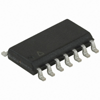
Manufacturer Part Number
ATTINY44-20SSU
Description
IC MCU AVR 4K FLASH 20MHZ 14SOIC
Manufacturer
Atmel
Series
AVR® ATtinyr
Specifications of ATTINY44-20SSU
Core Processor
AVR
Core Size
8-Bit
Speed
20MHz
Connectivity
USI
Peripherals
Brown-out Detect/Reset, POR, PWM, WDT
Number Of I /o
12
Program Memory Size
4KB (2K x 16)
Program Memory Type
FLASH
Eeprom Size
256 x 8
Ram Size
256 x 8
Voltage - Supply (vcc/vdd)
2.7 V ~ 5.5 V
Data Converters
A/D 8x10b
Oscillator Type
Internal
Operating Temperature
-40°C ~ 85°C
Package / Case
14-SOIC (3.9mm Width), 14-SOL
Cpu Family
ATtiny
Device Core
AVR
Device Core Size
8b
Frequency (max)
20MHz
Interface Type
SPI/USI
Total Internal Ram Size
256Byte
# I/os (max)
12
Number Of Timers - General Purpose
2
Operating Supply Voltage (typ)
3.3/5V
Operating Supply Voltage (max)
5.5V
Operating Supply Voltage (min)
2.7V
On-chip Adc
8-chx10-bit
Instruction Set Architecture
RISC
Operating Temp Range
-40C to 85C
Operating Temperature Classification
Industrial
Mounting
Surface Mount
Pin Count
14
Package Type
SOIC
For Use With
ATAVRISP2 - PROGRAMMER AVR IN SYSTEM
Lead Free Status / RoHS Status
Lead free / RoHS Compliant


10.1.2
10.1.3
10.1.4
56
ATtiny24/44/84
Toggling the Pin
Switching Between Input and Output
Reading the Pin Value
Writing a logic one to PINxn toggles the value of PORTxn, independent on the value of DDRxn.
Note that the SBI instruction can be used to toggle one single bit in a port.
When switching between tri-state ({DDxn, PORTxn} = 0b00) and output high ({DDxn, PORTxn}
= 0b11), an intermediate state with either pull-up enabled {DDxn, PORTxn} = 0b01) or output
low ({DDxn, PORTxn} = 0b10) must occur. Normally, the pull-up enabled state is fully accept-
able, as a high-impedant environment will not notice the difference between a strong high driver
and a pull-up. If this is not the case, the PUD bit in the MCUCR Register can be set to disable all
pull-ups in all ports.
Switching between input with pull-up and output low generates the same problem. The user
must use either the tri-state ({DDxn, PORTxn} = 0b00) or the output high state ({DDxn, PORTxn}
= 0b10) as an intermediate step.
Table 10-1
Table 10-1.
Independent of the setting of Data Direction bit DDxn, the port pin can be read through the
PINxn Register bit. As shown in
ing latch constitute a synchronizer. This is needed to avoid metastability if the physical pin
changes value near the edge of the internal clock, but it also introduces a delay.
shows a timing diagram of the synchronization when reading an externally applied pin value.
The maximum and minimum propagation delays are denoted t
Figure 10-3. Synchronization when Reading an Externally Applied Pin value
DDxn
0
0
0
1
1
PORTxn
summarizes the control signals for the pin value.
INSTRUCTIONS
0
1
1
0
1
Port Pin Configurations
SYSTEM CLK
SYNC LATCH
PINxn
(in MCUCR)
r17
PUD
X
X
X
0
1
Figure 10-2 on page
XXX
Output
Output
Input
Input
Input
I/O
t
pd, max
Pull-up
0x00
Yes
No
No
No
No
XXX
55, the PINxn Register bit and the preced-
t
pd, min
Comment
Tri-state (Hi-Z)
Pxn will source current if ext. pulled low
Tri-state (Hi-Z)
Output Low (Sink)
Output High (Source)
pd,max
in r17, PINx
and t
pd,min
0xFF
respectively.
8006K–AVR–10/10
Figure 10-3
Related parts for ATTINY44-20SSU
Image
Part Number
Description
Manufacturer
Datasheet
Request
R

Part Number:
Description:
Manufacturer:
Atmel Corporation
Datasheet:
Part Number:
Description:
Manufacturer:
Atmel Corporation
Datasheet:

Part Number:
Description:
MCU AVR 4K FLASH 15MHZ 20-QFN
Manufacturer:
Atmel
Datasheet:

Part Number:
Description:
IC MCU AVR 4K FLASH 20MHZ 20-QFN
Manufacturer:
Atmel
Datasheet:

Part Number:
Description:
MCU AVR 4KB FLASH 20MHZ 14SOIC
Manufacturer:
Atmel
Datasheet:
Part Number:
Description:
MCU AVR 4KB FLASH 20MHZ 20QFN
Manufacturer:
Atmel
Datasheet:

Part Number:
Description:
IC MCU AVR 4K FLASH 15MHZ 14SOIC
Manufacturer:
Atmel
Datasheet:

Part Number:
Description:
IC MCU AVR 4K FLASH 20MHZ 14-DIP
Manufacturer:
Atmel
Datasheet:
Part Number:
Description:
IC, MCU, 8BIT, 2K FLASH, 20SOIC
Manufacturer:
Atmel
Datasheet:

Part Number:
Description:
IC, MCU, 8BIT, 2K FLASH, 20PDIP
Manufacturer:
Atmel
Datasheet:
Part Number:
Description:
IC, MCU, 8BIT, 8K FLASH, 20PDIP
Manufacturer:
Atmel
Datasheet:
Part Number:
Description:
IC, MCU, 8BIT, 8K FLASH, 20SOIC
Manufacturer:
Atmel
Datasheet:

Part Number:
Description:
DEV KIT FOR AVR/AVR32
Manufacturer:
Atmel
Datasheet: