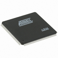
AT91M63200-25AU Atmel, AT91M63200-25AU Datasheet - Page 101

AT91M63200-25AU
Manufacturer Part Number
AT91M63200-25AU
Description
IC MCU ARM7 176-TQFP
Manufacturer
Atmel
Series
AT91SAMr
Datasheet
1.AT91M63200-25AI.pdf
(153 pages)
Specifications of AT91M63200-25AU
Core Processor
ARM7
Core Size
16/32-Bit
Speed
25MHz
Connectivity
EBI/EMI, SPI, UART/USART
Peripherals
POR, WDT
Number Of I /o
58
Program Memory Type
OTP
Ram Size
2K x 8
Voltage - Supply (vcc/vdd)
1.8 V ~ 3.6 V
Oscillator Type
External
Operating Temperature
-40°C ~ 85°C
Package / Case
176-TQFP, 176-VQFP
Lead Free Status / RoHS Status
Lead free / RoHS Compliant
Eeprom Size
-
Program Memory Size
-
Data Converters
-
Available stocks
Company
Part Number
Manufacturer
Quantity
Price
Company:
Part Number:
AT91M63200-25AU
Manufacturer:
NSC
Quantity:
1 670
SPI Mode Register
Register Name:
Access Type:
•
•
•
•
•
•
•
MSTR: Master/Slave Mode
0 = SPI is in Slave mode.
1 = SPI is in Master mode.
MSTR configures the SPI interface for either master or slave mode operation.
PS: Peripheral Select
0 = Fixed Peripheral Select.
1 = Variable Peripheral Select.
PCSDEC: Chip Select Decode
0 = The chip selects are directly connected to a peripheral device.
1 = The four chip select lines are connected to a 4- to 16-bit decoder.
When PCSDEC equals one, up to 16 chip select signals can be generated with the four lines using an external 4- to 16-
bit decoder.
The chip select registers define the characteristics of the 16 chip selects according to the following rules:
*Note: The 16th state corresponds to a state in which all chip selects are inactive. This allows a different clock configu-
ration to be defined by each chip select register.
MCK32: Clock Selection
0 = SPI master clock equals MCKI.
1 = SPI master clock equals MCKI/32.
LLB: Local Loopback Enable
0 = Local loopback path disabled.
1 = Local loopback path enabled.
LLB controls the local loopback on the data serializer for testing in master mode only.
PCS: Peripheral Chip Select
This field is only used if Fixed Peripheral Select is active (PS=0).
If PCSDEC=0:
If PCSDEC=1:
DLYBCS: Delay Between Chip Selects
This field defines the delay from NPCS inactive to the activation of another NPCS. The DLYBCS time guarantees non-
overlapping chip selects and solves bus contentions in case of peripherals having long data float times.
If DLYBCS is less than or equal to six, six SPI master clock periods will be inserted by default.
Otherwise, the following equation determines the delay:
LLB
31
23
15
SP_CSR0
SP_CSR1
SP_CSR2
SP_CSR3
PCS = xxx0
PCS = xx01
PCS = x011
PCS = 0111
PCS = 1111
(x = don’t care)
NPCS[3:0] output signals = PCS
–
–
7
Delay_ Between_Chip_Selects = DLYBCS * SPI_Master_Clock_period
30
22
14
SP_MR
Read/Write
–
–
6
–
defines peripheral chip select signals 0 to 3.
defines peripheral chip select signals 4 to 7.
defines peripheral chip select signals 8 to 11.
defines peripheral chip select signals 12 to 15*.
forbidden (no peripheral is selected)
NPCS[3:0] = 1110
NPCS[3:0] = 1101
NPCS[3:0] = 1011
NPCS[3:0] = 0111
29
21
13
–
–
5
–
28
20
12
–
–
4
–
DLYBCS
MCK32
27
19
11
–
3
PCSDEC
26
18
10
–
2
AT91M63200
PCS
PS
25
17
9
–
1
MSTR
24
16
8
–
0
101


