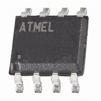
ATTINY11L-2SU Atmel, ATTINY11L-2SU Datasheet - Page 19

ATTINY11L-2SU
Manufacturer Part Number
ATTINY11L-2SU
Description
IC AVR MCU 1K FLASH 2MHZ 8SOIC
Manufacturer
Atmel
Series
AVR® ATtinyr
Specifications of ATTINY11L-2SU
Core Processor
AVR
Core Size
8-Bit
Speed
2MHz
Peripherals
WDT
Number Of I /o
6
Program Memory Size
1KB (512 x 16)
Program Memory Type
FLASH
Voltage - Supply (vcc/vdd)
2.7 V ~ 5.5 V
Oscillator Type
Internal
Operating Temperature
-40°C ~ 85°C
Package / Case
8-SOIC (5.3mm Width), 8-SOP, 8-SOEIAJ
Lead Free Status / RoHS Status
Lead free / RoHS Compliant
Eeprom Size
-
Ram Size
-
Data Converters
-
Connectivity
-
Other names
Q2525841
1006F–AVR–06/07
otherwise no EEPROM write takes place. The following procedure should be followed
when writing the EEPROM (the order of steps 2 and 3 is unessential):
1. Wait until EEWE becomes zero.
2. Write new EEPROM address to EEAR (optional).
3. Write new EEPROM data to EEDR (optional).
4. Write a logical one to the EEMWE bit in EECR (to be able to write a logical one
5. Within four clock cycles after setting EEMWE, write a logical one to EEWE.
Caution: An interrupt between step 4 and step 5 will make the write cycle fail, since the
EEPROM Master Write Enable will time-out. If an interrupt routine accessing the
EEPROM is interrupting another EEPROM access, the EEAR or EEDR register will be
modified, causing the interrupted EEPROM access to fail. It is recommended to have
the global interrupt flag cleared during the four last steps to avoid these problems.
When the write access time has elapsed, the EEWE bit is cleared (zero) by hardware.
The user software can poll this bit and wait for a zero before writing the next byte. When
EEWE has been set, the CPU is halted for two cycles before the next instruction is
executed.
• Bit 0 - EERE: EEPROM Read Enable
The EEPROM Read Enable Signal EERE is the read strobe to the EEPROM. When the
correct address is set up in the EEAR register, the EERE bit must be set. When the
EERE bit is cleared (zero) by hardware, requested data is found in the EEDR register.
The EEPROM read access takes one instruction and there is no need to poll the EERE
bit. When EERE has been set, the CPU is halted for four cycles before the next instruc-
tion is executed.
The user should poll the EEWE bit before starting the read operation. If a write operation
is in progress when new data or address is written to the EEPROM I/O registers, the
write operation will be interrupted, and the result is undefined.
The calibrated oscillator is used to time EEPROM. In Table 6 the typical programming
time is listed for EEPROM access from the CPU.
Table 6. Typical EEPROM Programming Times
Parameter
EEPROM write
to the EEMWE bit, the EEWE bit must be written to zero in the same cycle).
(from CPU)
Number of Calibrated
RC Oscillator Cycles
4096
Min Programming
Time
3.1 ms
ATtiny11/12
Max Programming
Time
6.8 ms
19


