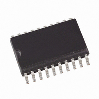
ATAM893T-TKQ Atmel, ATAM893T-TKQ Datasheet - Page 43

ATAM893T-TKQ
Manufacturer Part Number
ATAM893T-TKQ
Description
IC MON TIRE-PRESS ATARX9X SER
Manufacturer
Atmel
Series
MARC4r
Datasheet
1.ATAM893T-TKS.pdf
(98 pages)
Specifications of ATAM893T-TKQ
Core Processor
MARC4
Core Size
4-Bit
Speed
4MHz
Connectivity
SSI (2-Wire, 3 Wire)
Peripherals
Brown-out Detect/Reset, POR, PWM, WDT
Number Of I /o
16
Program Memory Size
4KB (4K x 8)
Program Memory Type
EEPROM
Eeprom Size
64 x 16
Ram Size
256 x 4
Voltage - Supply (vcc/vdd)
1.8 V ~ 6.5 V
Oscillator Type
Internal
Operating Temperature
-40°C ~ 125°C
Package / Case
20-SOIC (5.3mm Width), 20-SO, 20-SOEIAJ
Lead Free Status / RoHS Status
Contains lead / RoHS non-compliant
Data Converters
-
- Current page: 43 of 98
- Download datasheet (2Mb)
5.3.2.5
5.3.2.6
4680C–4BMCU–01/05
Timer 2 Control Register (T2C)
Timer 2 Mode Register 1 (T2M1)
Table 5-8.
Table 5-9.
T2C
T2CS1
T2CS0
T2TS
T2R
T2M1
T2D1
T2D0
T2MS1
T2MS0
T2D1
1
1
0
0
T2CS1
0
0
1
1
Bit 3
T2CS1
Timer 2 Clock Select bit 1
Timer 2 Clock Select bit 0
Timer 2 Toggle with Start
T2TS = 0, the output flip-flop of Timer 2 is not toggled with the timer start
T2TS = 1, the output flip-flop of Timer 2 is toggled when the timer is started with T2R
Timer 2 Run
T2R = 0, Timer 2 stop and reset
T2R = 1, Timer 2 run
Bit 3
T2D1
Timer 2 Duty cycle bit 1
Timer 2 Duty cycle bit 0
Timer 2 Mode Select bit 1
Timer 2 Mode Select bit 0
T2D0
Timer 2 Clock Select Bits
Timer 2 Duty Cycle Bits
1
0
1
0
Bit 2
T2D0
Bit 2
T2CS0
Function of Duty Cycle Generator (DCG)
Bypassed (DCGO0)
Duty cycle 1/1 (DCGO1)
Duty cycle 1/2 (DCGO2)
Duty cycle 1/3 (DCG03)
T2CS0
0
1
0
1
Bit 1
T2MS1
Bit 1
T2TS
Input Clock (CL 2/1) of Counter Stage 2/1
System clock (SYSCL)
Output signal of Timer 1 (T1OUT)
Internal shift clock of SSI (SCL)
Output signal of Timer 3 (TOG3)
Bit 0
T2MS0
Bit 0
T2R
Address: '7'hex — Subaddress: '1'hex
Reset value: 1111b
Address: '7'hex — Subaddress: '0'hex
Reset value: 0000b
Additional Divider Effect
ATAM893-D
/1
/2
/3
/4
43
Related parts for ATAM893T-TKQ
Image
Part Number
Description
Manufacturer
Datasheet
Request
R

Part Number:
Description:
IC MON TIRE-PRESS ATARX9X SER
Manufacturer:
Atmel
Datasheet:

Part Number:
Description:
IC MCU FLASH 4K MTP 20SSOP
Manufacturer:
Atmel
Datasheet:

Part Number:
Description:
flash, Microcontrollers, Microprocessors, Semiconductors and Actives, ic, mcu
Manufacturer:
Atmel
Datasheet:

Part Number:
Description:
Atam893-d Flash Version For Atar080, Atar090/890 And Atar092/892
Manufacturer:
ATMEL Corporation
Datasheet:

Part Number:
Description:
DEV KIT FOR AVR/AVR32
Manufacturer:
Atmel
Datasheet:

Part Number:
Description:
INTERVAL AND WIPE/WASH WIPER CONTROL IC WITH DELAY
Manufacturer:
ATMEL Corporation
Datasheet:

Part Number:
Description:
Low-Voltage Voice-Switched IC for Hands-Free Operation
Manufacturer:
ATMEL Corporation
Datasheet:

Part Number:
Description:
MONOLITHIC INTEGRATED FEATUREPHONE CIRCUIT
Manufacturer:
ATMEL Corporation
Datasheet:

Part Number:
Description:
AM-FM Receiver IC U4255BM-M
Manufacturer:
ATMEL Corporation
Datasheet:

Part Number:
Description:
Monolithic Integrated Feature Phone Circuit
Manufacturer:
ATMEL Corporation
Datasheet:

Part Number:
Description:
Multistandard Video-IF and Quasi Parallel Sound Processing
Manufacturer:
ATMEL Corporation
Datasheet:


