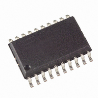
ATTINY2313-20SI Atmel, ATTINY2313-20SI Datasheet - Page 80

ATTINY2313-20SI
Manufacturer Part Number
ATTINY2313-20SI
Description
IC MCU AVR 2K FLASH 20SOIC
Manufacturer
Atmel
Series
AVR® ATtinyr
Specifications of ATTINY2313-20SI
Core Processor
AVR
Core Size
8-Bit
Speed
20MHz
Connectivity
SPI, UART/USART
Peripherals
Brown-out Detect/Reset, POR, PWM, WDT
Number Of I /o
18
Program Memory Size
2KB (1K x 16)
Program Memory Type
FLASH
Eeprom Size
128 x 8
Ram Size
128 x 8
Voltage - Supply (vcc/vdd)
2.7 V ~ 5.5 V
Oscillator Type
Internal
Operating Temperature
-40°C ~ 85°C
Package / Case
20-SOIC (7.5mm Width)
Lead Free Status / RoHS Status
Contains lead / RoHS non-compliant
Data Converters
-
Other names
ATTINY2313-24SI
ATTINY2313-24SI
ATTINY2313-24SI
Available stocks
Company
Part Number
Manufacturer
Quantity
Price
Company:
Part Number:
ATTINY2313-20SI
Manufacturer:
AT
Quantity:
95
Part Number:
ATTINY2313-20SI
Manufacturer:
RASTRONIC
Quantity:
20 000
- Current page: 80 of 226
- Download datasheet (4Mb)
Timer/Counter0
and
Timer/Counter1
Prescalers
Internal Clock Source
Prescaler Reset
External Clock Source
80
ATtiny2313
Timer/Counter1 and Timer/Counter0 share the same prescaler module, but the Timer/Counters
can have different prescaler settings. The description below applies to both Timer/Counter1 and
Timer/Counter0.
The Timer/Counter can be clocked directly by the system clock (by setting the CSn2:0 = 1). This
provides the fastest operation, with a maximum Timer/Counter clock frequency equal to system
clock frequency (f
clock source. The prescaled clock has a frequency of either f
f
The prescaler is free running, i.e., operates independently of the Clock Select logic of the
Timer/Counter, and it is shared by Timer/Counter1 and Timer/Counter0. Since the prescaler is
not affected by the Timer/Counter’s clock select, the state of the prescaler will have implications
for situations where a prescaled clock is used. One example of prescaling artifacts occurs when
the timer is enabled and clocked by the prescaler (6 > CSn2:0 > 1). The number of system clock
cycles from when the timer is enabled to the first count occurs can be from 1 to N+1 system
clock cycles, where N equals the prescaler divisor (8, 64, 256, or 1024).
It is possible to use the prescaler reset for synchronizing the Timer/Counter to program execu-
tion. However, care must be taken if the other Timer/Counter that shares the same prescaler
also uses prescaling. A prescaler reset will affect the prescaler period for all Timer/Counters it is
connected to.
An external clock source applied to the T1/T0 pin can be used as Timer/Counter clock
(clk
logic. The synchronized (sampled) signal is then passed through the edge detector.
shows a functional equivalent block diagram of the T1/T0 synchronization and edge detector
logic. The registers are clocked at the positive edge of the internal system clock (
is transparent in the high period of the internal system clock.
The edge detector generates one clk
(CSn2:0 = 6) edge it detects.
Figure 38. T1/T0 Pin Sampling
The synchronization and edge detector logic introduces a delay of 2.5 to 3.5 system clock cycles
from an edge has been applied to the T1/T0 pin to the counter is updated.
Enabling and disabling of the clock input must be done when T1/T0 has been stable for at least
one system clock cycle, otherwise it is a risk that a false Timer/Counter clock pulse is generated.
Each half period of the external clock applied must be longer than one system clock cycle to
ensure correct sampling. The external clock must be guaranteed to have less than half the sys-
tem clock frequency (f
sampling, the maximum frequency of an external clock it can detect is half the sampling fre-
CLK_I/O
T1
/clk
/1024.
Tn
clk
T0
I/O
). The T1/T0 pin is sampled once every system clock cycle by the pin synchronization
CLK_I/O
D
LE
ExtClk
Q
). Alternatively, one of four taps from the prescaler can be used as a
Synchronization
< f
D
clk_I/O
Q
/2) given a 50/50% duty cycle. Since the edge detector uses
T1
/clk
T
0
pulse for each positive (CSn2:0 = 7) or negative
D
CLK_I/O
Q
/8, f
CLK_I/O
Edge Detector
/64, f
clk
CLK_I/O
2543L–AVR–08/10
I/O
Tn_sync
(To Clock
Select Logic)
). The latch
Figure 38
/256, or
Related parts for ATTINY2313-20SI
Image
Part Number
Description
Manufacturer
Datasheet
Request
R

Part Number:
Description:
IC, MCU, 8BIT, 2K FLASH, 20SOIC
Manufacturer:
Atmel
Datasheet:

Part Number:
Description:
IC, MCU, 8BIT, 2K FLASH, 20PDIP
Manufacturer:
Atmel
Datasheet:

Part Number:
Description:
IC, MCU, 8BIT, 8K FLASH, 20PDIP
Manufacturer:
Atmel
Datasheet:

Part Number:
Description:
IC, MCU, 8BIT, 8K FLASH, 20SOIC
Manufacturer:
Atmel
Datasheet:

Part Number:
Description:
DEV KIT FOR AVR/AVR32
Manufacturer:
Atmel
Datasheet:

Part Number:
Description:
INTERVAL AND WIPE/WASH WIPER CONTROL IC WITH DELAY
Manufacturer:
ATMEL Corporation
Datasheet:

Part Number:
Description:
Low-Voltage Voice-Switched IC for Hands-Free Operation
Manufacturer:
ATMEL Corporation
Datasheet:

Part Number:
Description:
MONOLITHIC INTEGRATED FEATUREPHONE CIRCUIT
Manufacturer:
ATMEL Corporation
Datasheet:

Part Number:
Description:
AM-FM Receiver IC U4255BM-M
Manufacturer:
ATMEL Corporation
Datasheet:

Part Number:
Description:
Monolithic Integrated Feature Phone Circuit
Manufacturer:
ATMEL Corporation
Datasheet:

Part Number:
Description:
Multistandard Video-IF and Quasi Parallel Sound Processing
Manufacturer:
ATMEL Corporation
Datasheet:

Part Number:
Description:
High-performance EE PLD
Manufacturer:
ATMEL Corporation
Datasheet:


