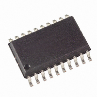
ATTINY2313-20SI Atmel, ATTINY2313-20SI Datasheet - Page 142

ATTINY2313-20SI
Manufacturer Part Number
ATTINY2313-20SI
Description
IC MCU AVR 2K FLASH 20SOIC
Manufacturer
Atmel
Series
AVR® ATtinyr
Specifications of ATTINY2313-20SI
Core Processor
AVR
Core Size
8-Bit
Speed
20MHz
Connectivity
SPI, UART/USART
Peripherals
Brown-out Detect/Reset, POR, PWM, WDT
Number Of I /o
18
Program Memory Size
2KB (1K x 16)
Program Memory Type
FLASH
Eeprom Size
128 x 8
Ram Size
128 x 8
Voltage - Supply (vcc/vdd)
2.7 V ~ 5.5 V
Oscillator Type
Internal
Operating Temperature
-40°C ~ 85°C
Package / Case
20-SOIC (7.5mm Width)
Lead Free Status / RoHS Status
Contains lead / RoHS non-compliant
Data Converters
-
Other names
ATTINY2313-24SI
ATTINY2313-24SI
ATTINY2313-24SI
Available stocks
Company
Part Number
Manufacturer
Quantity
Price
Company:
Part Number:
ATTINY2313-20SI
Manufacturer:
AT
Quantity:
95
Part Number:
ATTINY2313-20SI
Manufacturer:
RASTRONIC
Quantity:
20 000
- Current page: 142 of 226
- Download datasheet (4Mb)
Two-wire Mode
142
ATtiny2313
when the transfer is completed the data received from the Master is stored back into the r16
Register.
Note that the first two instructions is for initialization only and needs only to be executed
once.These instructions sets Three-wire mode and positive edge Shift Register clock. The loop
is repeated until the USI Counter Overflow Flag is set.
The USI Two-wire mode does not incorporate slew rate limiting on outputs and input noise filter-
ing. Pin names used by this mode are SCL and SDA.
Figure 63. Two-wire Mode Operation, Simplified Diagram
Figure 63
is only the physical layer that is shown since the system operation is highly dependent of the
communication scheme used. The main differences between the Master and Slave operation at
this level, is the serial clock generation which is always done by the Master, and only the Slave
uses the clock control unit. Clock generation must be implemented in software, but the shift
operation is done automatically by both devices. Note that only clocking on negative edge for
shifting data is of practical use in this mode. The slave can insert wait states at start or end of
transfer by forcing the SCL clock low. This means that the Master must always check if the SCL
line was actually released after it has generated a positive edge.
Since the clock also increments the counter, a counter overflow can be used to indicate that the
transfer is completed. The clock is generated by the master by toggling the USCK pin via the
PORT Register.
The data direction is not given by the physical layer. A protocol, like the one used by the TWI-
bus, must be implemented to control the data flow.
shows two USI units operating in Two-wire mode, one as Master and one as Slave. It
SLAVE
MASTER
Bit7
Bit7
Bit6
Bit6
Bit5
Bit5
Bit4
Bit4
Bit3
Bit3
Bit2
Bit2
Bit1
Bit1
Bit0
Bit0
Two-wire Clock
Control Unit
PORTxn
HOLD
SCL
SDA
SCL
SDA
SCL
VCC
2543L–AVR–08/10
Related parts for ATTINY2313-20SI
Image
Part Number
Description
Manufacturer
Datasheet
Request
R

Part Number:
Description:
IC, MCU, 8BIT, 2K FLASH, 20SOIC
Manufacturer:
Atmel
Datasheet:

Part Number:
Description:
IC, MCU, 8BIT, 2K FLASH, 20PDIP
Manufacturer:
Atmel
Datasheet:

Part Number:
Description:
IC, MCU, 8BIT, 8K FLASH, 20PDIP
Manufacturer:
Atmel
Datasheet:

Part Number:
Description:
IC, MCU, 8BIT, 8K FLASH, 20SOIC
Manufacturer:
Atmel
Datasheet:

Part Number:
Description:
DEV KIT FOR AVR/AVR32
Manufacturer:
Atmel
Datasheet:

Part Number:
Description:
INTERVAL AND WIPE/WASH WIPER CONTROL IC WITH DELAY
Manufacturer:
ATMEL Corporation
Datasheet:

Part Number:
Description:
Low-Voltage Voice-Switched IC for Hands-Free Operation
Manufacturer:
ATMEL Corporation
Datasheet:

Part Number:
Description:
MONOLITHIC INTEGRATED FEATUREPHONE CIRCUIT
Manufacturer:
ATMEL Corporation
Datasheet:

Part Number:
Description:
AM-FM Receiver IC U4255BM-M
Manufacturer:
ATMEL Corporation
Datasheet:

Part Number:
Description:
Monolithic Integrated Feature Phone Circuit
Manufacturer:
ATMEL Corporation
Datasheet:

Part Number:
Description:
Multistandard Video-IF and Quasi Parallel Sound Processing
Manufacturer:
ATMEL Corporation
Datasheet:

Part Number:
Description:
High-performance EE PLD
Manufacturer:
ATMEL Corporation
Datasheet:


