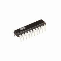
ATTINY26-16PJ Atmel, ATTINY26-16PJ Datasheet - Page 85

ATTINY26-16PJ
Manufacturer Part Number
ATTINY26-16PJ
Description
ID MCU AVR 2K 5V 16MHZ 20-DIP
Manufacturer
Atmel
Series
AVR® ATtinyr
Specifications of ATTINY26-16PJ
Core Processor
AVR
Core Size
8-Bit
Speed
16MHz
Connectivity
USI
Peripherals
Brown-out Detect/Reset, POR, PWM, WDT
Number Of I /o
16
Program Memory Size
2KB (1K x 16)
Program Memory Type
FLASH
Eeprom Size
128 x 8
Ram Size
128 x 8
Voltage - Supply (vcc/vdd)
4.5 V ~ 5.5 V
Data Converters
A/D 11x10b
Oscillator Type
Internal
Operating Temperature
-40°C ~ 85°C
Package / Case
20-DIP (0.300", 7.62mm)
Lead Free Status / RoHS Status
Lead free / RoHS Compliant
- Current page: 85 of 182
- Download datasheet (3Mb)
Functional
Descriptions
Three-wire Mode
1477K–AVR–08/10
The USI Three-wire mode is compliant to the Serial Peripheral Interface (SPI) mode 0 and 1, but
does not have the slave select (SS) pin functionality. However, this feature can be implemented
in software if necessary. Pin names used by this mode are: DI, DO, and SCK.
Figure 45. Three-wire Mode Operation, Simplified Diagram
Figure 45 shows two USI units operating in Three-wire mode, one as master and one as slave.
The two shift Registers are interconnected in such way that after eight SCK clocks, the data in
each register are interchanged. The same clock also increments the USI’s 4-bit counter. The
Counter Overflow (interrupt) flag, or USIOIF, can therefore be used to determine when a transfer
is completed. The clock is generated by the master device software by toggling the PB2 pin via
the PORTB Register or by writing a one to the USITC bit in USICR.
Figure 46. Three-wire Mode, Timing Diagram
The Three-wire mode timing is shown in Figure 46. At the top of the figure is a SCK cycle refer-
ence. One bit is shifted into the USI Shift Register (USIDR) for each of these cycles. The SCK
timing is shown for both external clock modes. In external clock mode 0 (USICS0 = 0), DI is
sampled at positive edges, and DO is changed (Data Register is shifted by one) at negative
edges. External clock mode 1 (USICS0 = 1) uses the opposite edges versus mode 0, i.e., sam-
CYCLE
SCK
SCK
SLAVE
MASTER
DO
DI
Bit7
Bit7
( Reference )
Bit6
Bit6
A
Bit5
Bit5
B
MSB
Bit4
Bit4
MSB
C
1
Bit3
Bit3
D
Bit2
Bit2
2
6
6
Bit1
Bit1
Bit0
Bit0
3
5
5
4
4
4
5
3
3
PORTBz
6
2
2
PBx
PBy
PBz
PBx
PBy
PBz
7
1
1
DO
DI
SCK
DO
DI
SCK
LSB
LSB
8
E
85
Related parts for ATTINY26-16PJ
Image
Part Number
Description
Manufacturer
Datasheet
Request
R

Part Number:
Description:
Manufacturer:
Atmel Corporation
Datasheet:

Part Number:
Description:
IC AVR MCU 2K 16MHZ IND 32-QFN
Manufacturer:
Atmel
Datasheet:

Part Number:
Description:
IC AVR MCU 2K 16MHZ IND 20-SOIC
Manufacturer:
Atmel
Datasheet:

Part Number:
Description:
IC AVR MCU 2K 16MHZ IND 20-DIP
Manufacturer:
Atmel
Datasheet:

Part Number:
Description:
IC AVR MCU 2K 16MHZ IND 32-QFN
Manufacturer:
Atmel
Datasheet:

Part Number:
Description:
IC AVR MCU 2K 16MHZ IND 20-DIP
Manufacturer:
Atmel
Datasheet:

Part Number:
Description:
IC AVR MCU 2K 16MHZ COM 20-SOIC
Manufacturer:
Atmel
Datasheet:

Part Number:
Description:
IC AVR MCU 2K 16MHZ IND 20-SOIC
Manufacturer:
Atmel
Datasheet:

Part Number:
Description:
ID MCU AVR 2K 5V 16MHZ 32-QFN
Manufacturer:
Atmel
Datasheet:

Part Number:
Description:
Microcontrollers (MCU) AVR 2K FLASH 128B EE 128B SRAM ADC
Manufacturer:
Atmel
Datasheet:

Part Number:
Description:
IC AVR MCU 2K 16MHZ COM 32-QFN
Manufacturer:
Atmel
Datasheet:

Part Number:
Description:
IC AVR MCU 2K 16MHZ COM 20-DIP
Manufacturer:
Atmel
Datasheet:

Part Number:
Description:
ID MCU AVR 2K 5V 16MHZ 20-SOIC
Manufacturer:
Atmel
Datasheet:

Part Number:
Description:
IC MCU AVR 2K 16MHZ IND 20SOIC
Manufacturer:
Atmel
Datasheet:


