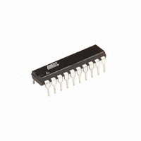
ATTINY26-16PJ Atmel, ATTINY26-16PJ Datasheet - Page 70

ATTINY26-16PJ
Manufacturer Part Number
ATTINY26-16PJ
Description
ID MCU AVR 2K 5V 16MHZ 20-DIP
Manufacturer
Atmel
Series
AVR® ATtinyr
Specifications of ATTINY26-16PJ
Core Processor
AVR
Core Size
8-Bit
Speed
16MHz
Connectivity
USI
Peripherals
Brown-out Detect/Reset, POR, PWM, WDT
Number Of I /o
16
Program Memory Size
2KB (1K x 16)
Program Memory Type
FLASH
Eeprom Size
128 x 8
Ram Size
128 x 8
Voltage - Supply (vcc/vdd)
4.5 V ~ 5.5 V
Data Converters
A/D 11x10b
Oscillator Type
Internal
Operating Temperature
-40°C ~ 85°C
Package / Case
20-DIP (0.300", 7.62mm)
Lead Free Status / RoHS Status
Lead free / RoHS Compliant
- Current page: 70 of 182
- Download datasheet (3Mb)
Timer/Counter1
Control Register A –
TCCR1A
70
ATtiny26(L)
• Bits 7, 6 – COM1A1, COM1A0: Comparator A Output Mode, Bits 1 and 0
The COM1A1 and COM1A0 control bits determine any output pin action following a Compare
Match with Compare Register A in Timer/Counter1. Output pin actions affect pin PB1 (OC1A).
Since this is an alternative function to an I/O port, the corresponding direction control bit must be
set (one) in order to control an output pin. Note that OC1A is not connected in normal mode.
Table 32. Comparator A Mode Select
In PWM mode, these bits have different functions. Refer to Table 35 on page 75 for a detailed
description.
• Bits 5, 4 – COM1B1, COM1B0: Comparator B Output Mode, Bits 1 and 0
The COM1B1 and COM1B0 control bits determine any output pin action following a Compare
Match with Compare Register B in Timer/Counter1. Output pin actions affect pin PB3 (OC1B).
Since this is an alternative function to an I/O port, the corresponding direction control bit must be
set (one) in order to control an output pin. Note that OC1B is not connected in normal mode.
Table 33. Comparator B Mode Select
In PWM mode, these bits have different functions. Refer to Table 35 on page 75 for a detailed
description.
• Bit 3 – FOC1A: Force Output Compare Match 1A
Writing a logical one to this bit forces a change in the Compare Match output pin PB1 (OC1A)
according to the values already set in COM1A1 and COM1A0. If COM1A1 and COM1A0 written
in the same cycle as FOC1A, the new settings will be used. The Force Output Compare bit can
be used to change the output pin value regardless of the timer value. The automatic action pro-
grammed in COM1A1 and COM1A0 takes place as if a compare match had occurred, but no
interrupt is generated. The FOC1A bit always reads as zero. FOC1A is not in use if PWM1A bit
is set.
• Bit 2 – FOC1B: Force Output Compare Match 1B
Writing a logical one to this bit forces a change in the Compare Match output pin PB3 (OC1B)
according to the values already set in COM1B1 and COM1B0. If COM1B1 and COM1B0 written
in the same cycle as FOC1B, the new settings will be used. The Force Output Compare bit can
Bit
$30 ($50)
Read/Write
Initial Value
COM1A1
COM1B1
0
0
1
1
0
0
1
1
COM1A1
R/W
COM1A0
COM1B0
7
0
0
1
0
1
0
1
0
1
COM1A0
R/W
6
0
Description
Timer/Counter Comparator A disconnected from output pin OC1A.
Toggle the OC1A output line.
Clear the OC1A output line.
Set the OC1A output line.
Description
Timer/Counter Comparator B disconnected from output pin OC1B.
Toggle the OC1B output line.
Clear the OC1B output line.
Set the OC1B output line.
COM1B1
R/W
5
0
COM1B0
R/W
4
0
FOC1A
R/W
3
0
FOC1B
R/W
2
0
PWM1A
R/W
1
0
PWM1B
R/W
0
0
TCCR1A
1477K–AVR–08/10
Related parts for ATTINY26-16PJ
Image
Part Number
Description
Manufacturer
Datasheet
Request
R

Part Number:
Description:
Manufacturer:
Atmel Corporation
Datasheet:

Part Number:
Description:
IC AVR MCU 2K 16MHZ IND 32-QFN
Manufacturer:
Atmel
Datasheet:

Part Number:
Description:
IC AVR MCU 2K 16MHZ IND 20-SOIC
Manufacturer:
Atmel
Datasheet:

Part Number:
Description:
IC AVR MCU 2K 16MHZ IND 20-DIP
Manufacturer:
Atmel
Datasheet:

Part Number:
Description:
IC AVR MCU 2K 16MHZ IND 32-QFN
Manufacturer:
Atmel
Datasheet:

Part Number:
Description:
IC AVR MCU 2K 16MHZ IND 20-DIP
Manufacturer:
Atmel
Datasheet:

Part Number:
Description:
IC AVR MCU 2K 16MHZ COM 20-SOIC
Manufacturer:
Atmel
Datasheet:

Part Number:
Description:
IC AVR MCU 2K 16MHZ IND 20-SOIC
Manufacturer:
Atmel
Datasheet:

Part Number:
Description:
ID MCU AVR 2K 5V 16MHZ 32-QFN
Manufacturer:
Atmel
Datasheet:

Part Number:
Description:
Microcontrollers (MCU) AVR 2K FLASH 128B EE 128B SRAM ADC
Manufacturer:
Atmel
Datasheet:

Part Number:
Description:
IC AVR MCU 2K 16MHZ COM 32-QFN
Manufacturer:
Atmel
Datasheet:

Part Number:
Description:
IC AVR MCU 2K 16MHZ COM 20-DIP
Manufacturer:
Atmel
Datasheet:

Part Number:
Description:
ID MCU AVR 2K 5V 16MHZ 20-SOIC
Manufacturer:
Atmel
Datasheet:

Part Number:
Description:
IC MCU AVR 2K 16MHZ IND 20SOIC
Manufacturer:
Atmel
Datasheet:


