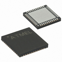
ATMEGA8535L-8MI Atmel, ATMEGA8535L-8MI Datasheet - Page 128

ATMEGA8535L-8MI
Manufacturer Part Number
ATMEGA8535L-8MI
Description
IC AVR MCU 8K LV 8MHZ IND 44-QFN
Manufacturer
Atmel
Series
AVR® ATmegar
Specifications of ATMEGA8535L-8MI
Core Processor
AVR
Core Size
8-Bit
Speed
8MHz
Connectivity
I²C, SPI, UART/USART
Peripherals
Brown-out Detect/Reset, POR, PWM, WDT
Number Of I /o
32
Program Memory Size
8KB (4K x 16)
Program Memory Type
FLASH
Eeprom Size
512 x 8
Ram Size
512 x 8
Voltage - Supply (vcc/vdd)
2.7 V ~ 5.5 V
Data Converters
A/D 8x10b
Oscillator Type
Internal
Operating Temperature
-40°C ~ 85°C
Package / Case
44-VQFN Exposed Pad
Data Bus Width
8 bit
Data Ram Size
512 B
Interface Type
SPI, TWI, UART
Maximum Clock Frequency
8 MHz
Number Of Programmable I/os
32
Number Of Timers
3
Operating Supply Voltage
2.7 V to 5.5 V
Maximum Operating Temperature
+ 85 C
Mounting Style
SMD/SMT
Minimum Operating Temperature
- 40 C
On-chip Adc
10 bit, 8 Channel
Lead Free Status / RoHS Status
Contains lead / RoHS non-compliant
Available stocks
Company
Part Number
Manufacturer
Quantity
Price
Company:
Part Number:
ATMEGA8535L-8MI
Manufacturer:
SanRex
Quantity:
1 000
- Current page: 128 of 321
- Download datasheet (3Mb)
8-bit Timer/Counter
Register Description
Timer/Counter Control
Register – TCCR2
128
ATmega8535(L)
Figure 63. Timer/Counter Timing Diagram, Clear Timer on Compare Match Mode, with
Prescaler (f
• Bit 7 – FOC2: Force Output Compare
The FOC2 bit is only active when the WGM bits specify a non-PWM mode. However, for
ensuring compatibility with future devices, this bit must be set to zero when TCCR2 is
written when operating in PWM mode. When writing a logical one to the FOC2 bit, an
immediate Compare Match is forced on the Waveform Generation unit. The OC2 output
is changed according to its COM21:0 bits setting. Note that the FOC2 bit is implemented
as a strobe. Therefore it is the value present in the COM21:0 bits that determines the
effect of the forced compare.
A FOC2 strobe will not generate any interrupt, nor will it clear the timer in CTC mode
using OCR2 as TOP.
The FOC2 bit is always read as zero.
• Bit 6, 3 – WGM21:0: Waveform Generation Mode
These bits control the counting sequence of the counter, the source for the maximum
(TOP) counter value, and what type of waveform generation to be used. Modes of oper-
ation supported by the Timer/Counter unit are: Normal mode, Clear Timer on Compare
Match (CTC) mode, and two types of Pulse Width Modulation (PWM) modes. See Table
51 and “Modes of Operation” on page 122.
TCNTn
(clk
Bit
Read/Write
Initial Value
OCRn
(CTC)
OCFn
clk
clk
I/O
I/O
Tn
/8)
clk_I/O
FOC2
W
7
0
/8)
TOP - 1
WGM20
R/W
6
0
COM21
R/W
5
0
COM20
R/W
TOP
4
0
WGM21
TOP
R/W
3
0
CS22
R/W
BOTTOM
2
0
CS21
R/W
1
0
CS20
R/W
0
0
2502K–AVR–10/06
BOTTOM + 1
TCCR2
Related parts for ATMEGA8535L-8MI
Image
Part Number
Description
Manufacturer
Datasheet
Request
R

Part Number:
Description:
IC AVR MCU 2.4GHZ XCEIVER 64QFN
Manufacturer:
Atmel
Datasheet:

Part Number:
Description:
Manufacturer:
Atmel
Datasheet:

Part Number:
Description:
MCU ATMEGA644/AT86RF230 40-DIP
Manufacturer:
Atmel
Datasheet:

Part Number:
Description:
BUNDLE ATMEGA644P/AT86RF230 QFN
Manufacturer:
Atmel
Datasheet:

Part Number:
Description:
BUNDLE ATMEGA644P/AT86RF230 TQFP
Manufacturer:
Atmel
Datasheet:

Part Number:
Description:
MCU ATMEGA1281/AT86RF230 64-TQFP
Manufacturer:
Atmel
Datasheet:

Part Number:
Description:
MCU ATMEGA1280/AT86RF230 100TQFP
Manufacturer:
Atmel
Datasheet:

Part Number:
Description:
BUNDLE ATMEGA1280/AT86RF100-TQFP
Manufacturer:
Atmel
Datasheet:

Part Number:
Description:
BUNDLE ATMEGA2560V/AT86RF230-ZU
Manufacturer:
Atmel
Datasheet:

Part Number:
Description:
MCU ATMEGA2561/AT86RF230 64-TQFP
Manufacturer:
Atmel
Datasheet:

Part Number:
Description:
INTERVAL AND WIPE/WASH WIPER CONTROL IC WITH DELAY
Manufacturer:
ATMEL Corporation
Datasheet:

Part Number:
Description:
Low-Voltage Voice-Switched IC for Hands-Free Operation
Manufacturer:
ATMEL Corporation
Datasheet:

Part Number:
Description:
MONOLITHIC INTEGRATED FEATUREPHONE CIRCUIT
Manufacturer:
ATMEL Corporation
Datasheet:

Part Number:
Description:
AM-FM Receiver IC U4255BM-M
Manufacturer:
ATMEL Corporation
Datasheet:


