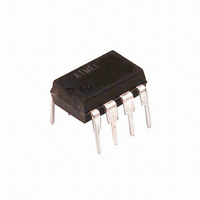
ATTINY11L-2PI Atmel, ATTINY11L-2PI Datasheet - Page 36

ATTINY11L-2PI
Manufacturer Part Number
ATTINY11L-2PI
Description
IC AVR MCU 1K 2MHZ LV IND 8-DIP
Manufacturer
Atmel
Series
AVR® ATtinyr
Specifications of ATTINY11L-2PI
Core Processor
AVR
Core Size
8-Bit
Speed
2MHz
Peripherals
WDT
Number Of I /o
6
Program Memory Size
1KB (512 x 16)
Program Memory Type
FLASH
Voltage - Supply (vcc/vdd)
2.7 V ~ 5.5 V
Oscillator Type
Internal
Operating Temperature
-40°C ~ 85°C
Package / Case
8-DIP (0.300", 7.62mm)
Lead Free Status / RoHS Status
Contains lead / RoHS non-compliant
Eeprom Size
-
Ram Size
-
Data Converters
-
Connectivity
-
Other names
ATTINY11L2PI
Available stocks
Company
Part Number
Manufacturer
Quantity
Price
Part Number:
ATTINY11L-2PI
Manufacturer:
ATMEL/爱特梅尔
Quantity:
20 000
I/O Port B
36
ATtiny11/12
All AVR ports have true read-modify-write functionality when used as general digital I/O
ports. This means that the direction of one port pin can be changed without unintention-
ally changing the direction of any other pin with the SBI and CBI instructions. The same
applies for changing drive value (if configured as output) or enabling/disabling of pull-up
resistors (if configured as input).
Port B is a 6-bit bi-directional I/O port.
Three I/O memory address locations are allocated for Port B, one each for the Data
Register – PORTB, $18, Data Direction Register – DDRB, $17, and the Port B Input
Pins – PINB, $16. The Port B Input Pins address is read only, while the Data Register
and the Data Direction Register are read/write.
Ports PB5..3 have special functions as described in the section “Pin Descriptions” on
page 5. If PB5 is not configured as external reset, it is input with no pull-up. On
ATtiny12, it can also output a logical zero, acting as an open-drain output. Note that,
since PB5 only has one possible output value, the output functionality of this pin is con-
trolled by the DDRB register alone. If PB4 and/or PB3 are not used for clock function,
they are I/O pins. All I/O pins have individually selectable pull-ups.
The Port B output buffers on PB0 to PB4 can sink 20 mA and thus drive LED displays
directly. On ATtiny12, PB5 can sink 12 mA. When pins PB0 to PB4 are used as inputs
and are externally pulled low, they will source current (I
activated.
The Port B pins with alternate functions are shown in Table 16:
Table 16. Port B Pins Alternate Functions
When the pins PB2..0 are used for the alternate function, the DDRB and PORTB regis-
ter has to be set according to the alternate function description. When PB5..3 are used
for alternate functions, the values in the corresponding DDRB and PORTB bits are
ignored.
Port Pin
PB0
PB1
PB2
PB3
PB4
PB5
Alternate Functions
AIN0 (Analog Comparator Positive Input)
MOSI (Data Input Line for Memory Downloading)
INT0 (External Interrupt0 Input)
AIN1 (Analog Comparator Negative Input)
MISO (Data Output Line for Memory Downloading)
T0 (Timer/Counter0 External Counter Input)
SCK (Serial Clock Input for Serial Programming)
XTAL1 (Oscillator Input)
XTAL2 (Oscillator Output)
RESET (External Reset Pin)
IL
) if the internal pull-ups are
Device
ATtiny11/12
ATtiny12
ATtiny11/12
ATtiny11/12
ATtiny12
ATtiny11/12
ATtiny12
ATtiny11/12
ATtiny11/12
ATtiny11/12
1006F–AVR–06/07


