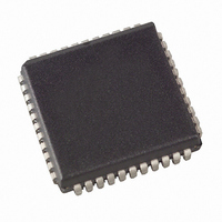
AT89LS53-12JI Atmel, AT89LS53-12JI Datasheet - Page 14

AT89LS53-12JI
Manufacturer Part Number
AT89LS53-12JI
Description
IC 8051 MCU FLASH 12K 44PLCC
Manufacturer
Atmel
Series
89LSr
Datasheet
1.AT89LS53-12AC.pdf
(35 pages)
Specifications of AT89LS53-12JI
Core Processor
8051
Core Size
8-Bit
Speed
12MHz
Connectivity
SPI, UART/USART
Peripherals
POR, WDT
Number Of I /o
32
Program Memory Size
12KB (12K x 8)
Program Memory Type
FLASH
Ram Size
256 x 8
Voltage - Supply (vcc/vdd)
2.7 V ~ 6 V
Oscillator Type
Internal
Operating Temperature
-40°C ~ 85°C
Package / Case
44-PLCC
Lead Free Status / RoHS Status
Contains lead / RoHS non-compliant
Eeprom Size
-
Data Converters
-
Other names
AT89LS5312JI
Available stocks
Company
Part Number
Manufacturer
Quantity
Price
Company:
Part Number:
AT89LS53-12JI
Manufacturer:
ATMEL
Quantity:
1 831
Part Number:
AT89LS53-12JI
Manufacturer:
ATMEL/爱特梅尔
Quantity:
20 000
Programmable Clock Out
A 50% duty cycle clock can be programmed to come out on
P1.0, as shown in Figure 5. This pin, besides being a regu-
lar I/0 pin, has two alternate functions. It can be pro-
grammed to input the external clock for Timer/Counter 2 or
to output a 50% duty cycle clock ranging from 61 Hz to 3
MHz at a 12 MHz operating frequency.
To configure the Timer/Counter 2 as a clock generator, bit
C/T2 (T2CON.1) must be cleared and bit T2OE (T2MOD.1)
must be set. Bit TR2 (T2CON.2) starts and stops the timer.
The clock-out frequency depends on the oscillator fre-
quency and the reload value of Timer 2 capture registers
(RCAP2H, RCAP2L), as shown in the following equation.
In the clock-out mode, Timer 2 rollovers will not generate
an interrupt. This behavior is similar to when Timer 2 is
used as a baud-rate generator. It is possible to use Timer 2
as a baud-rate generator and a clock generator simulta-
neously. Note, however, that the baud-rate and clock-out
frequencies cannot be determined independently from one
another since they both use RCAP2H and RCAP2L.
Figure 6. SPI Block Diagram
14
Clock-Out Frequency
AT89LS53
=
SPI STATUS REGISTER
OSCILLATOR
÷4÷16÷64÷128
------------------------------------------------------------------------------------------ -
4
SELECT
DIVIDER
×
SPI CONTROL
[
65536
Oscillator Frequency
SPI INTERRUPT
–
SPI CLOCK (MASTER)
(
REQUEST
RCAP2H,RCAP2L
MSTR
SPE
8
INTERNAL
MSB
DATA BUS
8/16-BIT SHIFT REGISTER
8
READ DATA BUFFER
)
]
8
SPI CONTROL REGISTER
UART
The UART in the AT89LS53 operates the same way as the
UART in the AT89C51, AT89C52 and AT89C55. For fur-
ther information, see the October 1995 Atmel Microcontrol-
ler Data Book, page 2-49, section titled, “Serial Interface.”
Serial Peripheral Interface
The serial peripheral interface (SPI) allows high-speed syn-
chronous data transfer between the AT89LS53 and periph-
eral devices or between several AT89LS53 devices. The
AT89LS53 SPI features include the following:
• Full-Duplex, 3-Wire Synchronous Data Transfer
• Master or Slave Operation
• 1.5-MHz Bit Frequency (max.)
• LSB First or MSB First Data Transfer
• Four Programmable Bit Rates
• End of Transmission Interrupt Flag
• Write Collision Flag Protection
• Wakeup from Idle Mode (Slave Mode Only)
CLOCK
LOGIC
LSB
CLOCK
S
M
M
S
S
M
MISO
MOSI
P1.6
P1.5
SCK
P1.4
1.7
SS
0851C–MICRO–3/06


