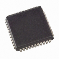
AT89S53-24JI Atmel, AT89S53-24JI Datasheet - Page 8

AT89S53-24JI
Manufacturer Part Number
AT89S53-24JI
Description
MICRO CONTROLLER
Manufacturer
Atmel
Series
89Sr
Datasheet
1.AT89S53-24JI.pdf
(35 pages)
Specifications of AT89S53-24JI
Core Processor
8051
Core Size
8-Bit
Speed
24MHz
Connectivity
SPI, UART/USART
Peripherals
WDT
Number Of I /o
32
Program Memory Size
12KB (12K x 8)
Program Memory Type
FLASH
Ram Size
256 x 8
Voltage - Supply (vcc/vdd)
4 V ~ 6 V
Oscillator Type
Internal
Operating Temperature
-40°C ~ 85°C
Package / Case
44-PLCC
Data Bus Width
8 bit
Data Ram Size
256 B
Interface Type
SPI, UART
Maximum Clock Frequency
24 MHz
Number Of Programmable I/os
32
Number Of Timers
3 x 16 bit
Operating Supply Voltage
4 V to 6 V
Maximum Operating Temperature
+ 85 C
Mounting Style
SMD/SMT
Minimum Operating Temperature
- 40 C
Lead Free Status / RoHS Status
Contains lead / RoHS non-compliant
Eeprom Size
-
Data Converters
-
Lead Free Status / Rohs Status
No
Other names
Q1036833
Available stocks
Company
Part Number
Manufacturer
Quantity
Price
Company:
Part Number:
AT89S53-24JI
Manufacturer:
ATM
Quantity:
620
Company:
Part Number:
AT89S53-24JI
Manufacturer:
ATM
Quantity:
620
Part Number:
AT89S53-24JI
Manufacturer:
ATMEL/爱特梅尔
Quantity:
20 000
Table 4. SPCR—SPI Control Register
Table 5. SPSR—SPI Status Register Data Memory - RAM
Table 6. SPDR—SPI Data Register
8
SPCR Address = D5H
Symbol
SPIE
SPE
DORD
MSTR
CPOL
CPHA
SPR0
SPR1
SPSR Address = AAH
Symbol
SPIF
WCOL
SPDR Address = 86H
Bit
Bit
Bit
AT89S53
SPIE
SPIF
SPD7
Function
SPI Interrupt Enable. This bit, in conjunction with the ES bit in the IE register, enables SPI interrupts: SPIE = 1 and ES
= 1 enable SPI interrupts. SPIE = 0 disables SPI interrupts.
SPI Enable. SPI = 1 enables the SPI channel and connects SS, MOSI, MISO and SCK to pins P1.4, P1.5, P1.6, and
P1.7. SPI = 0 disables the SPI channel.
Data Order. DORD = 1 selects LSB first data transmission. DORD = 0 selects MSB first data transmission.
Master/Slave Select. MSTR = 1 selects Master SPI mode. MSTR = 0 selects Slave SPI mode.
Clock Polarity. When CPOL = 1, SCK is high when idle. When CPOL = 0, SCK of the master device is low when not
transmitting. Please refer to figure on SPI Clock Phase and Polarity Control.
Clock Phase. The CPHA bit together with the CPOL bit controls the clock and data relationship between master and
slave. Please refer to figure on SPI Clock Phase and Polarity Control.
SPI Clock Rate Select. These two bits control the SCK rate of the device configured as master. SPR1 and SPR0 have
no effect on the slave. The relationship between SCK and the oscillator frequency, F
SPR1SPR0SCK = F
Function
SPI Interrupt Flag. When a serial transfer is complete, the SPIF bit is set and an interrupt is generated if SPIE = 1 and
ES = 1. The SPIF bit is cleared by reading the SPI status register with SPIF and WCOL bits set, and then accessing
the SPI data register.
Write Collision Flag. The WCOL bit is set if the SPI data register is written during a data transfer. During data transfer,
the result of reading the SPDR register may be incorrect, and writing to it has no effect. The WCOL bit (and the SPIF
bit) are cleared by reading the SPI status register with SPIF and WCOL set, and then accessing the SPI data register.
7
7
7
0
0
1
1
0
1 16
0 64
1 128
4
WCOL
SPE
SPD6
6
6
6
OSC.
divided by
DORD
SPD5
5
–
5
5
MSTR
SPD4
4
–
4
4
CPOL
SPD3
3
–
3
3
CPHA
SPD2
2
–
2
2
OSC.
Reset Value = 00XX XXXXB
Reset Value = 0000 01XXB
SPR1
Reset Value = unchanged
, is as follows:
SPD1
1
–
1
1
SPR0
SPD0
0
–
0
0
0787E–MICRO–3/06


