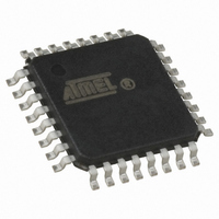
AT90S4433-8AC Atmel, AT90S4433-8AC Datasheet - Page 54

AT90S4433-8AC
Manufacturer Part Number
AT90S4433-8AC
Description
IC MCU 4K FLSH 8MHZ A/D 32TQFP
Manufacturer
Atmel
Series
AVR® 90Sr
Datasheet
1.AT90S4433-8AC.pdf
(126 pages)
Specifications of AT90S4433-8AC
Core Processor
AVR
Core Size
8-Bit
Speed
8MHz
Connectivity
SPI, UART/USART
Peripherals
Brown-out Detect/Reset, POR, PWM, WDT
Number Of I /o
20
Program Memory Size
4KB (2K x 16)
Program Memory Type
FLASH
Eeprom Size
256 x 8
Ram Size
128 x 8
Voltage - Supply (vcc/vdd)
4 V ~ 6 V
Data Converters
A/D 6x10b
Oscillator Type
External
Operating Temperature
0°C ~ 70°C
Package / Case
32-TQFP, 32-VQFP
Lead Free Status / RoHS Status
Contains lead / RoHS non-compliant
Available stocks
Company
Part Number
Manufacturer
Quantity
Price
Part Number:
AT90S4433-8AC
Manufacturer:
ATMEL/爱特梅尔
Quantity:
20 000
data is transferred from UDR to the 10(11)-bit Shift Register, bit 0 of the Shift Register is
cleared (start bit) and bit 9 or 10 is set (stop bit). If 9-bit data word is selected (the CHR9
bit in the UART Control and Status Register B, UCSRB is set), the TXB8 bit in UCSRB is
transferred to bit nine in the Transmit Shift Register.
On the baud rate clock following the transfer operation to the Shift Register, the start bit
is shifted out on the TXD pin. Then follows the data, LSB first. When the stop bit has
been shifted out, the Shift Register is loaded if any new data has been written to the
UDR during the transmission. During loading, UDRE is set. If there is no new data in the
UDR Register to send when the stop bit is shifted out, the UDRE Flag will remain set
until UDR is written again. When no new data has been written, and the stop bit has
been present on TXD for one bit length, the TX Complete Flag, TXC, in UCSRA is set.
The TXEN bit in UCSRB enables the UART Transmitter when set (one). When this bit is
cleared (zero), the PD1 pin can be used for general I/O. When TXEN is set, the UART
Transmitter will be connected to PD1, which is forced to be an output pin regardless of
the setting of the DDD1 bit in DDRD.
Data Reception
Figure 41 shows a block diagram of the UART Receiver.
Figure 41. UART Receiver
UART CONTROL
UART CONTROL
AND STAUS
AND STAUS
REGISTER A (UCSRA)
REGISTER B (UCSRB)
AT90S/LS4433
54
1042H–AVR–04/03


