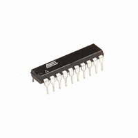
AT90S2313-4PI Atmel, AT90S2313-4PI Datasheet - Page 31

AT90S2313-4PI
Manufacturer Part Number
AT90S2313-4PI
Description
IC MCU 2K 4MHZ UART LV IT 20DIP
Manufacturer
Atmel
Series
AVR® 90Sr
Datasheet
1.AT90S2313-10PC.pdf
(92 pages)
Specifications of AT90S2313-4PI
Core Processor
AVR
Core Size
8-Bit
Speed
4MHz
Connectivity
SPI, UART/USART
Peripherals
Brown-out Detect/Reset, POR, PWM, WDT
Number Of I /o
15
Program Memory Size
2KB (1K x 16)
Program Memory Type
FLASH
Eeprom Size
128 x 8
Ram Size
128 x 8
Voltage - Supply (vcc/vdd)
2.7 V ~ 6 V
Oscillator Type
External
Operating Temperature
-40°C ~ 85°C
Package / Case
20-DIP (0.300", 7.62mm)
Lead Free Status / RoHS Status
Contains lead / RoHS non-compliant
Data Converters
-
Available stocks
Company
Part Number
Manufacturer
Quantity
Price
Company:
Part Number:
AT90S2313-4PI
Manufacturer:
ATMEL
Quantity:
5 530
Part Number:
AT90S2313-4PI
Manufacturer:
ATMEL/爱特梅尔
Quantity:
20 000
Timer/Counter1 Control
Register A – TCCR1A
0839I–AVR–06/02
Timer/Counter1 can also be used as an 8-, 9-, or 10-bit Pulse Width Modulator. In this
mode the counter and the OCR1 Register serve as a glitch-free standalone PWM with
centered pulses. Refer to page 35 for a detailed description of this function.
The Input Capture function of Timer/Counter1 provides a capture of the Timer/Counter1
contents to the Input Capture Register (ICR1), triggered by an external event on the
Input Capture Pin (ICP). The actual capture event settings are defined by the
Timer/Counter1 Control Register (TCCR1B). In addition, the Analog Comparator can be
set to trigger the input capture. Refer to “Analog Comparator” on page 48 for details on
this. The ICP pin logic is shown in Figure 31.
Figure 31. ICP Pin Schematic Diagram
If the Noise Canceler function is enabled, the actual trigger condition for the capture
event is monitored over four samples, and all four must be equal to activate the capture
flag.
• Bits 7, 6 – COM1A1, COM1A0: Compare Output Mode1, Bits 1 and 0
The COM1A1 and COM1A0 control bits determine any output pin action following a
compare match in Timer/Counter1. Any output pin actions affect pin OC1 (Output Com-
pare pin 1) (PB3). This is an alternative function to the I/O port, and the corresponding
direction control bit must be set (one) to control an output pin. The control configuration
is shown in Table 8.
Table 8. Compare 1 Mode Select
Notes:
• Bits 5..2 – Res: Reserved Bits
These bits are reserved bits in the AT90S2313 and always read zero.
Bit
$2F ($4F)
Read/Write
Initial value
COM1A1
0
0
1
1
1. In PWM mode, these bits have a different function. Refer to Table 12 for a detailed
2. The initial state of the OC1 output line is undefined.
description.
COM1A1
R/W
0
7
COM1A0
0
1
0
1
COM1A0
R/W
6
0
Description
Timer/Counter1 disconnected from output pin OC1
Toggle the OC1 output line.
Clear the OC1 output line (to zero).
Set the OC1 output line (to one).
R
5
–
0
(1)(2)
R
4
–
0
R
3
–
0
R
2
–
0
PWM11
R/W
AT90S2313
1
0
PWM10
R/W
0
0
TCCR1A
31


