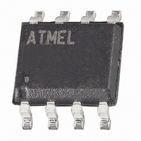
AT90LS2323-4SI Atmel, AT90LS2323-4SI Datasheet - Page 43

AT90LS2323-4SI
Manufacturer Part Number
AT90LS2323-4SI
Description
IC MCU 2K FLASH 4MHZ LV 8-SOIC
Manufacturer
Atmel
Series
AVR® 90LSr
Datasheet
1.AT90LS2323-4PC.pdf
(64 pages)
Specifications of AT90LS2323-4SI
Core Processor
AVR
Core Size
8-Bit
Speed
4MHz
Connectivity
SPI
Peripherals
Brown-out Detect/Reset, POR, WDT
Number Of I /o
3
Program Memory Size
2KB (1K x 16)
Program Memory Type
FLASH
Eeprom Size
128 x 8
Ram Size
128 x 8
Voltage - Supply (vcc/vdd)
2.7 V ~ 6 V
Oscillator Type
Internal
Operating Temperature
-40°C ~ 85°C
Package / Case
8-SOIC (5.3mm Width), 8-SOP, 8-SOEIAJ
Lead Free Status / RoHS Status
Contains lead / RoHS non-compliant
Data Converters
-
Available stocks
Company
Part Number
Manufacturer
Quantity
Price
Part Number:
AT90LS2323-4SI
Manufacturer:
ATMEL/爱特梅尔
Quantity:
20 000
Low-voltage Serial
Programming Algorithm
1004D–09/01
For the EEPROM, an auto-erase cycle is provided within the self-timed Write instruction
and there is no need to first execute the Chip Erase instruction. The Chip Erase instruc-
tion turns the content of every memory location in both the program and EEPROM
arrays into $FF.
The program and EEPROM memory arrays have separate address spaces: $0000 to
$03FF for Flash program memory and $000 to $07F for EEPROM data memory.
Either an external clock is applied to the XTAL1/PB3 pin or the device must be clocked
from the internal RC oscillator (AT90S/LS2343 only). The minimum low and high peri-
ods for the serial clock (SCK) input are defined as follows:
When writing serial data to the AT90S2323/2343, data is clocked on the rising edge of
SCK.
When reading data from the AT90S2323/2343, data is clocked on the falling edge of
SCK. See Figure 36, Figure 37 and Table 20 for timing details.
To program and verify the AT90S2323/2343 in the low-voltage Serial Programming
mode, the following sequence is recommended (see 4-byte instruction formats in
Table 19):
1. Power-up sequence:
2. Wait for at least 20 ms and enable serial programming by sending the Program-
3. The serial programming instructions will not work if the communication is out of
4. If a Chip Erase is performed (must be done to erase the Flash), wait t
5. The Flash or EEPROM array is programmed one byte at a time by supplying the
6. Any memory location can be verified by using the Read instruction, which returns
Low: > 2 MCU clock cycles
High: > 2 MCU clock cycles
Apply power between V
programmer cannot guarantee that SCK is held low during power-up, RESET must
be given a positive pulse after SCK has been set to “0”.) If the device is pro-
grammed for external clocking, apply a 0 - 8 MHz clock to the XTAL1/PB3 pin. If the
internal RC oscillator is selected as the clock source, no external clock source
needs to be applied (AT90S/LS2343 only).
ming Enable serial instruction to the MOSI (PB0) pin. Refer to the above section
for minimum low and high periods for the serial clock input, SCK.
synchronization. When in sync, the second byte ($53) will echo back when issu-
ing the third byte of the Programming Enable instruction. Whether the echo is
correct or not, all four bytes of the instruction must be transmitted. If the $53 did
not echo back, give SCK a positive pulse and issue a new Programming Enable
instruction. If the $53 is not seen within 32 attempts, there is no functional device
connected.
after the instruction, give RESET a positive pulse and start over from step 2. See
Table 21 on page 46 for t
address and data together with the appropriate Write instruction. An EEPROM
memory location is first automatically erased before new data is written. Use
Data Polling to detect when the next byte in the Flash or EEPROM can be writ-
ten. If polling is not used, wait t
See Table 22 on page 46 for t
data file(s) need to be programmed.
the content at the selected address at the serial output MISO (PB1) pin.
CC
WD_ERASE
and GND while RESET and SCK are set to “0”. (If the
WD_PROG
WD_PROG
value.
value. In an erased device, no $FFs in the
before transmitting the next instruction.
AT90S/LS2323/2343
WD_ERASE
43


