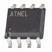
AT90LS2323-4SI Atmel, AT90LS2323-4SI Datasheet - Page 36

AT90LS2323-4SI
Manufacturer Part Number
AT90LS2323-4SI
Description
IC MCU 2K FLASH 4MHZ LV 8-SOIC
Manufacturer
Atmel
Series
AVR® 90LSr
Datasheet
1.AT90LS2323-4PC.pdf
(64 pages)
Specifications of AT90LS2323-4SI
Core Processor
AVR
Core Size
8-Bit
Speed
4MHz
Connectivity
SPI
Peripherals
Brown-out Detect/Reset, POR, WDT
Number Of I /o
3
Program Memory Size
2KB (1K x 16)
Program Memory Type
FLASH
Eeprom Size
128 x 8
Ram Size
128 x 8
Voltage - Supply (vcc/vdd)
2.7 V ~ 6 V
Oscillator Type
Internal
Operating Temperature
-40°C ~ 85°C
Package / Case
8-SOIC (5.3mm Width), 8-SOP, 8-SOEIAJ
Lead Free Status / RoHS Status
Contains lead / RoHS non-compliant
Data Converters
-
Available stocks
Company
Part Number
Manufacturer
Quantity
Price
Part Number:
AT90LS2323-4SI
Manufacturer:
ATMEL/爱特梅尔
Quantity:
20 000
Port B Input Pins Address –
PINB
Port B as General Digital
I/O
Alternate Functions of Port B
36
AT90S/LS2323/2343
The Port B Input Pins address (PINB) is not a register and this address enables access
to the physical value on each Port B pin. When reading PORTB, the Port B Data Latch
is read and when reading PINB, the logical values present on the pins are read.
All pins in port B have equal functionality when used as digital I/O pins.
PBn, general I/O pin: The DDBn bit in the DDRB register selects the direction of this pin,
if DDBn is set (one), PBn is configured as an output pin. If DDBn is cleared (zero), PBn
is configured as an input pin. If PORTBn is set (one) when the pin is configured as an
input pin, the MOS pull-up resistor is activated. To switch the pull-up resistor off, the
PORTBn has to be cleared (zero) or the pin has to be configured as an output pin. The
port pins are tri-stated when a reset condition becomes active, even if the clock is not
running.
Table 13. DDBn Effects on Port B Pins
The alternate pin functions of Port B are as follows:
• CLOCK – Port B, Bit 3
Clock input: AT90S/LS2343 only. When the RCEN fuse is programmed and the device
runs from the internal RC oscillator, this pin is a general I/O pin. When the RCEN fuse is
unprogrammed, an external clock source must be connected to CLOCK.
• SCK/T0 – Port B, Bit 2
In Serial Programming mode, this bit serves as the serial clock input, SCK.
During normal operation, this pin can serve as the external counter clock input. See the
timer/counter description for further details. If external timer/counter clocking is selected,
activity on this pin will clock the counter even if it is configured as an output.
• MISO/INT0 – Port B, Bit 1
In Serial Programming mode, this bit serves as the serial data output, MISO.
During normal operation, this pin can serve as the external interrupt0 input. See the
interrupt description for details on how to enable this interrupt. Note that activity on this
pin will trigger the interrupt even if the pin is configured as an output.
• MOSI – Port B, Bit 0
In Serial Programming mode, this pin serves as the serial data input, MOSI.
Bit
$16 ($36)
Read/Write
Initial Value
DDBn
0
0
1
1
PORTBn
R
7
–
0
0
1
0
1
R
6
–
0
Output
Output
Input
Input
I/O
R
0
5
–
Pull-up
Yes
No
No
No
PINB4
N/A
R
4
Comment
Tri-state (high-Z)
PBn will source current if ext. pulled low
Push-pull Zero Output
Push-pull One Output
PINB3
N/A
R
3
PINB2
N/A
R
2
PINB1
N/A
R
1
PINB0
N/A
R
0
1004D–09/01
PINB


