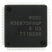
M30873FHGP#U3 Renesas Electronics America, M30873FHGP#U3 Datasheet - Page 293

M30873FHGP#U3
Manufacturer Part Number
M30873FHGP#U3
Description
IC M32C/87 MCU FLASH 100LQFP
Manufacturer
Renesas Electronics America
Series
M16C™ M32C/80r
Datasheet
1.M3087BFLGPU3.pdf
(629 pages)
Specifications of M30873FHGP#U3
Core Processor
M32C/80
Core Size
16/32-Bit
Speed
32MHz
Connectivity
CAN, EBI/EMI, I²C, IEBus, IrDA, SIO, UART/USART
Peripherals
DMA, POR, PWM, WDT
Number Of I /o
85
Program Memory Size
384KB (384K x 8)
Program Memory Type
FLASH
Ram Size
24K x 8
Voltage - Supply (vcc/vdd)
3 V ~ 5.5 V
Data Converters
A/D 26x10b; D/A 2x8b
Oscillator Type
Internal
Operating Temperature
-40°C ~ 85°C
Package / Case
100-LQFP
For Use With
R0K330879S001BE - KIT DEV RSK M32C/87R0K330879S000BE - KIT DEV RSK M32C/87
Lead Free Status / RoHS Status
Lead free / RoHS Compliant
Eeprom Size
-
Available stocks
Company
Part Number
Manufacturer
Quantity
Price
- Current page: 293 of 629
- Download datasheet (16Mb)
M32C/87 Group (M32C/87, M32C/87A, M32C/87B)
REJ09B0180-0151 Rev.1.51 Jul 31, 2008
Page 269 of 587
Figure 17.37
17.1.7
Table 17.21
“0” output pulse width
“0” input pulse width
I/O polarity
f1
f8
Input and output data in clock asynchronous mode are converted into the format supporting IrDA physical layer
specification v.1.0. The UART0 transmit data is encoded and output in the RZI (Return to Zero Inverted)
format. Input data in the RZI format is decoded to the NRZ (None Return to Zero) format and becomes the
UART0 reception input data. Refer to the 17.1.2 Clock Asynchronous (UART) Mode for details on clock
asynchronous mode.
Table 17.21 lists specifications of IrDA mode. Figure 17.37 shows a block diagram. Figure 17.38 shows a
register associated with IrDA mode. Figure 17.39 shows an IrDA operation.
0
1
UART0
Module
IRCK
Special Mode 5 (IrDA mode) • • • UART0
Item
IrDA Mode Specifications
IrDA Mode Block Diagram
U0BRG clock
Internal transmit clock
Transmission output
Internal receive clock
Reception input
1/2
1/2
• PLSSEL bit in the IRCON register is set to 0 (3/16 of the bit rate)
• PLSSEL bit is set to 1 (set by bits IRPD0, IRPD1, IRCK)
Input the pulse which is longer than
Encode logic “0” to a high pulse, decode a high pulse as logic “0”
Encode logic “0” to a low pulse, decode a low pulse as logic “0”
Selectable among
16
3
1/2
IRSEL
bit time
IRPD1 and IRPD0
00
01
10
11
1
0
Pulse Decoder
Pulse Encoder
1
0
1
fi , fi , fi , fi
PLSSEL
2
4
IRRPOL
Specification
8
3
fi
0
1
0
1
17. Serial Interfaces (UART0 to UART4)
IRTPOL
fi = f1 or f8
Eliminate the pulse shorter than
1
0
Filter
IRSEL
TXD0/IrDAOUT
RXD0/IrDAIN
3
fi
Related parts for M30873FHGP#U3
Image
Part Number
Description
Manufacturer
Datasheet
Request
R

Part Number:
Description:
KIT STARTER FOR M16C/29
Manufacturer:
Renesas Electronics America
Datasheet:

Part Number:
Description:
KIT STARTER FOR R8C/2D
Manufacturer:
Renesas Electronics America
Datasheet:

Part Number:
Description:
R0K33062P STARTER KIT
Manufacturer:
Renesas Electronics America
Datasheet:

Part Number:
Description:
KIT STARTER FOR R8C/23 E8A
Manufacturer:
Renesas Electronics America
Datasheet:

Part Number:
Description:
KIT STARTER FOR R8C/25
Manufacturer:
Renesas Electronics America
Datasheet:

Part Number:
Description:
KIT STARTER H8S2456 SHARPE DSPLY
Manufacturer:
Renesas Electronics America
Datasheet:

Part Number:
Description:
KIT STARTER FOR R8C38C
Manufacturer:
Renesas Electronics America
Datasheet:

Part Number:
Description:
KIT STARTER FOR R8C35C
Manufacturer:
Renesas Electronics America
Datasheet:

Part Number:
Description:
KIT STARTER FOR R8CL3AC+LCD APPS
Manufacturer:
Renesas Electronics America
Datasheet:

Part Number:
Description:
KIT STARTER FOR RX610
Manufacturer:
Renesas Electronics America
Datasheet:

Part Number:
Description:
KIT STARTER FOR R32C/118
Manufacturer:
Renesas Electronics America
Datasheet:

Part Number:
Description:
KIT DEV RSK-R8C/26-29
Manufacturer:
Renesas Electronics America
Datasheet:

Part Number:
Description:
KIT STARTER FOR SH7124
Manufacturer:
Renesas Electronics America
Datasheet:

Part Number:
Description:
KIT STARTER FOR H8SX/1622
Manufacturer:
Renesas Electronics America
Datasheet:

Part Number:
Description:
KIT DEV FOR SH7203
Manufacturer:
Renesas Electronics America
Datasheet:


