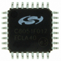
C8051F017-GQ Silicon Laboratories Inc, C8051F017-GQ Datasheet - Page 20

C8051F017-GQ
Manufacturer Part Number
C8051F017-GQ
Description
IC 8051 MCU 32K FLASH 32LQFP
Manufacturer
Silicon Laboratories Inc
Series
C8051F01xr
Specifications of C8051F017-GQ
Program Memory Type
FLASH
Program Memory Size
32KB (32K x 8)
Package / Case
32-LQFP
Core Processor
8051
Core Size
8-Bit
Speed
25MHz
Connectivity
SMBus (2-Wire/I²C), SPI, UART/USART
Peripherals
Brown-out Detect/Reset, POR, PWM, Temp Sensor, WDT
Number Of I /o
8
Ram Size
2.25K x 8
Voltage - Supply (vcc/vdd)
2.7 V ~ 3.6 V
Data Converters
A/D 4x10b; D/A 2x12b
Oscillator Type
Internal
Operating Temperature
-40°C ~ 85°C
Processor Series
C8051F0x
Core
8051
Data Bus Width
8 bit
Data Ram Size
2.25 KB
Interface Type
I2C/SMBus/SPI/UART
Maximum Clock Frequency
25 MHz
Number Of Programmable I/os
8
Number Of Timers
4
Operating Supply Voltage
2.7 V to 3.6 V
Maximum Operating Temperature
+ 85 C
Mounting Style
SMD/SMT
3rd Party Development Tools
PK51, CA51, A51, ULINK2
Development Tools By Supplier
C8051F005DK
Minimum Operating Temperature
- 40 C
On-chip Adc
4-ch x 10-bit
On-chip Dac
2-ch x 12-bit
No. Of I/o's
8
Ram Memory Size
256Byte
Cpu Speed
25MHz
No. Of Timers
4
No. Of Pwm Channels
5
Rohs Compliant
Yes
Lead Free Status / RoHS Status
Lead free / RoHS Compliant
Eeprom Size
-
Lead Free Status / Rohs Status
Lead free / RoHS Compliant
Other names
336-1196
Available stocks
Company
Part Number
Manufacturer
Quantity
Price
Company:
Part Number:
C8051F017-GQ
Manufacturer:
Silicon Labs
Quantity:
135
Company:
Part Number:
C8051F017-GQ
Manufacturer:
Silicon Laboratories Inc
Quantity:
10 000
Company:
Part Number:
C8051F017-GQR
Manufacturer:
Silicon Laboratories Inc
Quantity:
10 000
2. ABSOLUTE MAXIMUM RATINGS*
Ambient temperature under bias................................................................................................................. -55 to 125C
Storage Temperature .................................................................................................................................. -65 to 150C
Voltage on any Pin (except VDD and Port I/O) with respect to DGND ................................... -0.3V to (VDD + 0.3V)
Voltage on any Port I/O Pin or /RST with respect to DGND....................................................................-0.3V to 5.8V
Voltage on VDD with respect to DGND...................................................................................................-0.3V to 4.2V
Maximum Total current through VDD, AV+, DGND and AGND .....................................................................800mA
Maximum output current sunk by any Port pin ...................................................................................................100mA
Maximum output current sunk by any other I/O pin .............................................................................................25mA
Maximum output current sourced by any Port pin ..............................................................................................100mA
Maximum output current sourced by any other I/O pin ........................................................................................25mA
*Note: Stresses above those listed under “Absolute Maximum Ratings” may cause permanent damage to the device.
This is a stress rating only and functional operation of the devices at those or any other conditions above those
indicated in the operation listings of this specification is not implied. Exposure to maximum rating conditions for
extended periods may affect device reliability.
3. GLOBAL DC ELECTRICAL CHARACTERISTICS
-40C to +85C unless otherwise specified.
Analog Supply Voltage
Analog Supply Current
Analog Supply Current with
analog sub-systems inactive
Analog-to-Digital Supply
Delta ( | VDD – AV+ | )
Digital Supply Voltage
Digital Supply Current with
CPU active
Digital Supply Current
(shutdown)
Digital Supply RAM Data
Retention Voltage
Specified Operating
Temperature Range
SYSCLK (System Clock
Frequency)
SYSCLK (System Clock
Frequency)
Tsysl (SYSCLK Low Time)
Tsysh (SYSCLK High Time)
Note 1: Analog Supply AV+ must be greater than 1V for VDD monitor to operate.
Note 2: SYSCLK must be at least 32 kHz to enable debugging.
PARAMETER
(Note 1)
Internal REF, ADC, DAC, Comparators
all active
Internal REF, ADC, DAC, Comparators
all disabled, oscillator disabled
VDD = 2.7V, Clock=25MHz
VDD = 2.7V, Clock=1MHz
VDD = 2.7V, Clock=32kHz
Oscillator not running
C8051F005/6/7, C8051F015/6/7
(Note 2)
C8051F000/1/2, C8051F010/1/2
(Note 2)
CONDITIONS
Rev. 1.7
C8051F000/1/2/5/6/7
C8051F010/1/2/5/6/7
MIN
-40
2.7
2.7
18
18
0
0
TYP
12.5
3.0
3.0
0.5
1.5
10
1
5
5
MAX
+85
3.6
0.5
3.6
20
25
20
2
UNITS
MHz
MHz
mA
mA
mA
A
A
A
C
ns
ns
V
V
V
V
20


