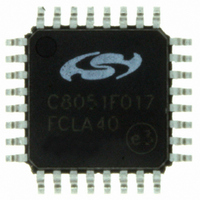
C8051F017-GQ Silicon Laboratories Inc, C8051F017-GQ Datasheet - Page 16

C8051F017-GQ
Manufacturer Part Number
C8051F017-GQ
Description
IC 8051 MCU 32K FLASH 32LQFP
Manufacturer
Silicon Laboratories Inc
Series
C8051F01xr
Specifications of C8051F017-GQ
Program Memory Type
FLASH
Program Memory Size
32KB (32K x 8)
Package / Case
32-LQFP
Core Processor
8051
Core Size
8-Bit
Speed
25MHz
Connectivity
SMBus (2-Wire/I²C), SPI, UART/USART
Peripherals
Brown-out Detect/Reset, POR, PWM, Temp Sensor, WDT
Number Of I /o
8
Ram Size
2.25K x 8
Voltage - Supply (vcc/vdd)
2.7 V ~ 3.6 V
Data Converters
A/D 4x10b; D/A 2x12b
Oscillator Type
Internal
Operating Temperature
-40°C ~ 85°C
Processor Series
C8051F0x
Core
8051
Data Bus Width
8 bit
Data Ram Size
2.25 KB
Interface Type
I2C/SMBus/SPI/UART
Maximum Clock Frequency
25 MHz
Number Of Programmable I/os
8
Number Of Timers
4
Operating Supply Voltage
2.7 V to 3.6 V
Maximum Operating Temperature
+ 85 C
Mounting Style
SMD/SMT
3rd Party Development Tools
PK51, CA51, A51, ULINK2
Development Tools By Supplier
C8051F005DK
Minimum Operating Temperature
- 40 C
On-chip Adc
4-ch x 10-bit
On-chip Dac
2-ch x 12-bit
No. Of I/o's
8
Ram Memory Size
256Byte
Cpu Speed
25MHz
No. Of Timers
4
No. Of Pwm Channels
5
Rohs Compliant
Yes
Lead Free Status / RoHS Status
Lead free / RoHS Compliant
Eeprom Size
-
Lead Free Status / Rohs Status
Lead free / RoHS Compliant
Other names
336-1196
Available stocks
Company
Part Number
Manufacturer
Quantity
Price
Company:
Part Number:
C8051F017-GQ
Manufacturer:
Silicon Labs
Quantity:
135
Company:
Part Number:
C8051F017-GQ
Manufacturer:
Silicon Laboratories Inc
Quantity:
10 000
Company:
Part Number:
C8051F017-GQR
Manufacturer:
Silicon Laboratories Inc
Quantity:
10 000
1.4.
The standard 8051 Ports (0, 1, 2, and 3) are available on the MCUs. All four ports are pinned out on the
F000/05/10/15. Ports 0 and 1 are pinned out on the F001/06/11/16, and only Port 0 is pinned out on the
F002/07/12/17. The Ports not pinned out are still available for software use as general purpose registers. The Port
I/O behave like the standard 8051 with a few enhancements.
Each Port I/O pin can be configured as either a push-pull or open-drain output. Also, the “weak pull-ups” which are
normally fixed on an 8051 can be globally disabled, providing additional power saving capabilities for low power
applications.
Perhaps the most unique enhancement is the Digital Crossbar. This is essentially a large digital switching network
that allows mapping of internal digital system resources to Port I/O pins on P0, P1, and P2. (See Figure 1.8.)
Unlike microcontrollers with standard multiplexed digital I/O, all combinations of functions are supported.
The on-board counter/timers, serial buses, HW interrupts, ADC Start of Conversion input, comparator outputs, and
other digital signals in the controller can be configured to appear on the Port I/O pins specified in the Crossbar
Control registers. This allows the user to select the exact mix of general purpose Port I/O and digital resources
needed for his particular application.
Programmable Digital I/O and Crossbar
Highest
Priority
Lowest
Priority
Latches
Port
SYSCLK
CNVSTR
Comptr.
Outputs
SMBus
T0, T1,
UART
P0
P1
P2
P3
PCA
SPI
Figure 1.8. Digital Crossbar Diagram
T2
(P0.0-P0.7)
(P1.0-P1.7)
(P2.0-P2.7)
(P3.0-P3.7)
8
8
8
8
2
4
2
6
2
6
Rev. 1.7
XBR2 Registers
XBR0, XBR1,
Crossbar
Decoder
Priority
Digital
8
8
8
PRT0CF, PRT1CF,
PRT2CF Registers
PRT3CF
Register
Cells
Cells
Cells
Cells
P0
I/O
P1
I/O
P2
I/O
P3
I/O
C8051F000/1/2/5/6/7
C8051F010/1/2/5/6/7
External
Pins
P0.0
P0.7
P1.0
P1.7
P2.0
P2.7
P3.0
P3.7
Highest
Priority
Lowest
Priority
16


