R5F21237JFP Renesas Electronics America, R5F21237JFP Datasheet - Page 153
R5F21237JFP
Manufacturer Part Number
R5F21237JFP
Description
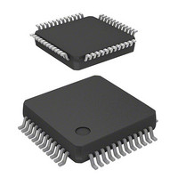
MCU 3/5V 48K+2K 48-LQFP
Manufacturer
Renesas Electronics America
Series
R8C/2x/23r
Datasheet
1.R5F21237DFPU0.pdf
(551 pages)
Specifications of R5F21237JFP
Core Processor
R8C
Core Size
16/32-Bit
Speed
20MHz
Connectivity
CAN, I²C, LIN, SIO, SSU, UART/USART
Peripherals
POR, Voltage Detect, WDT
Number Of I /o
41
Program Memory Size
48KB (48K x 8)
Program Memory Type
FLASH
Ram Size
2.5K x 8
Voltage - Supply (vcc/vdd)
2.7 V ~ 5.5 V
Data Converters
A/D 12x10b
Oscillator Type
Internal
Operating Temperature
-40°C ~ 85°C
Package / Case
48-LQFP
For Use With
RCDK8C - KIT DEV EVAL FOR CAN R8C/23R0E521237CPE00 - EMULATOR COMPACT R8C/20/21/22/23
Lead Free Status / RoHS Status
Lead free / RoHS Compliant
Eeprom Size
-
Available stocks
Company
Part Number
Manufacturer
Quantity
Price
Company:

Part Number:
R5F21237JFP
Manufacturer:
Renesas Electronics America
Quantity:
10 000
Part Number:
R5F21237JFP
Manufacturer:
RENESAS/瑞萨
Quantity:
20 000
Company:
Part Number:
R5F21237JFP#ES
Manufacturer:
Renesas Electronics America
Quantity:
10 000
Company:
Part Number:
R5F21237JFP#U1
Manufacturer:
Renesas Electronics America
Quantity:
10 000
Company:
Part Number:
R5F21237JFP#V0
Manufacturer:
Renesas Electronics America
Quantity:
10 000


R8C/22 Group, R8C/23 Group
Rev.2.00 Aug 20, 2008
REJ09B0251-0200
Figure 14.2
Timer RA I/O Control Register
Timer RA Control Register
b7 b6 b5 b4
NOTES:
b7 b6 b5 b4 b3 b2
1.
2.
3.
4.
5.
Refer to 14.1.6 Notes on Tim er RA .
When the TSTOP bit is set to 1, bits TSTART and TCSTF and registers TRAPRE and TRA are set to the values after a
reset.
Bits TEDGF and TUNDF can be set to 0 by w riting 0 to these bits by a program. How ever, their value remains
unchanged w hen 1 is w ritten.
In pulse w idth measurement mode and pulse period measurement mode, use the MOV instruction to set the TRACR
register. If it is necessary to avoid changing the values of bits TEDGF and TUNDF, w rite 1 to them.
Set to 0 in timer mode, pulse output mode, and event counter mode.
b3 b2
b1 b0
b1 b0
Registers TRACR and TRAIOC
Bit Symbol
Bit Symbol
TEDGSEL
TSTART
TRAIOC
(b7-b6)
TOENA
TIOSEL
(b7-b6)
Symbol
TRACR
TSTOP
TEDGF
TUNDF
Symbol
TOPCR
TCSTF
TIPF0
TIPF1
Page 131 of 501
(b3)
—
—
—
(4)
TRAIO polarity sw itch bit
TRAIO output control bit
TRAO output enable bit
_____
INT1
TRAIO input filter select bits
Nothing is assigned. If necessary, set to 0.
When read, the content is 0.
Timer RA count start bit
Timer RA count status flag
Timer RA count forcible stop
bit
Nothing is assigned. If necessary, set to 0.
When read, the content is 0.
Active edge reception
flag
Timer RA underflow flag
Nothing is assigned. If necessary, set to 0.
When read, the content is 0.
(2)
(3,5)
/TRAIO select bit
Address
Bit Name
Address
Bit Name
0100h
0101h
(1)
(3,5)
(1)
Function varies depending on operation mode
0 : Stops counting
1 : Starts counting
0 : Stops counting
1 : Counting
When this bit is set to 1, the count is forcibly
stopped. When read, the content is 0.
0 : Active edge not received
1 : Active edge received
0 : No underflow
1 : Underflow
(end of measurement period)
After Reset
After Reset
Function
Function
00h
00h
14. Timers
RW
RW
RW
RW
RW
RW
RW
RW
RW
RW
RW
RW
RO
—
—
—
Related parts for R5F21237JFP
Image
Part Number
Description
Manufacturer
Datasheet
Request
R

Part Number:
Description:
KIT STARTER FOR M16C/29
Manufacturer:
Renesas Electronics America
Datasheet:

Part Number:
Description:
KIT STARTER FOR R8C/2D
Manufacturer:
Renesas Electronics America
Datasheet:

Part Number:
Description:
R0K33062P STARTER KIT
Manufacturer:
Renesas Electronics America
Datasheet:

Part Number:
Description:
KIT STARTER FOR R8C/23 E8A
Manufacturer:
Renesas Electronics America
Datasheet:

Part Number:
Description:
KIT STARTER FOR R8C/25
Manufacturer:
Renesas Electronics America
Datasheet:

Part Number:
Description:
KIT STARTER H8S2456 SHARPE DSPLY
Manufacturer:
Renesas Electronics America
Datasheet:

Part Number:
Description:
KIT STARTER FOR R8C38C
Manufacturer:
Renesas Electronics America
Datasheet:

Part Number:
Description:
KIT STARTER FOR R8C35C
Manufacturer:
Renesas Electronics America
Datasheet:

Part Number:
Description:
KIT STARTER FOR R8CL3AC+LCD APPS
Manufacturer:
Renesas Electronics America
Datasheet:
Part Number:
Description:
KIT STARTER FOR RX610
Manufacturer:
Renesas Electronics America
Datasheet:

Part Number:
Description:
KIT STARTER FOR R32C/118
Manufacturer:
Renesas Electronics America
Datasheet:

Part Number:
Description:
KIT DEV RSK-R8C/26-29
Manufacturer:
Renesas Electronics America
Datasheet:

Part Number:
Description:
KIT STARTER FOR SH7124
Manufacturer:
Renesas Electronics America
Datasheet:

Part Number:
Description:
KIT STARTER FOR H8SX/1622
Manufacturer:
Renesas Electronics America
Datasheet:

Part Number:
Description:
KIT DEV FOR SH7203
Manufacturer:
Renesas Electronics America
Datasheet: