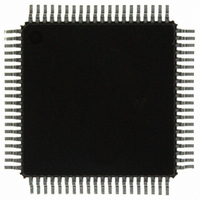
MC9S12C96CFUE Freescale Semiconductor, MC9S12C96CFUE Datasheet - Page 373

MC9S12C96CFUE
Manufacturer Part Number
MC9S12C96CFUE
Description
IC MCU 96K FLASH 4K RAM 80-QFP
Manufacturer
Freescale Semiconductor
Series
HCS12r
Specifications of MC9S12C96CFUE
Core Processor
HCS12
Core Size
16-Bit
Speed
25MHz
Connectivity
CAN, EBI/EMI, SCI, SPI
Peripherals
POR, PWM, WDT
Number Of I /o
60
Program Memory Size
96KB (96K x 8)
Program Memory Type
FLASH
Ram Size
4K x 8
Voltage - Supply (vcc/vdd)
2.35 V ~ 5.5 V
Data Converters
A/D 8x10b
Oscillator Type
Internal
Operating Temperature
-40°C ~ 85°C
Package / Case
80-QFP
Processor Series
S12C
Core
HCS12
Data Bus Width
16 bit
Data Ram Size
4 KB
Interface Type
CAN/SCI/SPI
Maximum Clock Frequency
25 MHz
Number Of Programmable I/os
60
Number Of Timers
8
Operating Supply Voltage
- 0.3 V to + 6.5 V
Maximum Operating Temperature
+ 85 C
Mounting Style
SMD/SMT
3rd Party Development Tools
EWHCS12
Development Tools By Supplier
M68EVB912C32EE
Minimum Operating Temperature
- 40 C
On-chip Adc
8-ch x 10-bit
Lead Free Status / RoHS Status
Lead free / RoHS Compliant
Eeprom Size
-
Lead Free Status / Rohs Status
Lead free / RoHS Compliant
Available stocks
Company
Part Number
Manufacturer
Quantity
Price
Company:
Part Number:
MC9S12C96CFUE
Manufacturer:
Freescale Semiconductor
Quantity:
10 000
Company:
Part Number:
MC9S12C96CFUER
Manufacturer:
Freescale Semiconductor
Quantity:
10 000
- Current page: 373 of 690
- Download datasheet (4Mb)
12.4.1.2
The scaled A clock uses clock A as an input and divides it further with a user programmable value and
then divides this by 2. The scaled B clock uses clock B as an input and divides it further with a user
programmable value and then divides this by 2. The rates available for clock SA are software selectable
to be clock A divided by 2, 4, 6, 8, ..., or 512 in increments of divide by 2. Similar rates are available for
clock SB.
Clock A is used as an input to an 8-bit down counter. This down counter loads a user programmable scale
value from the scale register (PWMSCLA). When the down counter reaches 1, two things happen; a pulse
is output and the 8-bit counter is re-loaded. The output signal from this circuit is further divided by two.
This gives a greater range with only a slight reduction in granularity. Clock SA equals clock A divided by
two times the value in the PWMSCLA register.
Similarly, clock B is used as an input to an 8-bit down counter followed by a divide by two producing clock
SB. Thus, clock SB equals clock B divided by two times the value in the PWMSCLB register.
As an example, consider the case in which the user writes 0x00FF into the PWMSCLA register. Clock A
for this case will be bus clock divided by 4. A pulse will occur at a rate of once every 255 x 4 bus cycles.
Passing this through the divide by two circuit produces a clock signal at a bus clock divided by 2040 rate.
Similarly, a value of 0x0001 in the PWMSCLA register when clock A is bus clock divided by 4 will
produce a bus clock divided by 8 rate.
Writing to PWMSCLA or PWMSCLB causes the associated 8-bit down counter to be re-loaded.
Otherwise, when changing rates the counter would have to count down to 0x0001 before counting at the
proper rate. Forcing the associated counter to re-load the scale register value every time PWMSCLA or
PWMSCLB is written prevents this.
Freescale Semiconductor
Clock Scale
Clock SA = Clock A / (2 * PWMSCLA)
When PWMSCLA = 0x0000, PWMSCLA value is considered a full scale
value of 256. Clock A is thus divided by 512.
Clock SB = Clock B / (2 * PWMSCLB)
When PWMSCLB = 0x0000, PWMSCLB value is considered a full scale
value of 256. Clock B is thus divided by 512.
Writing to the scale registers while channels are operating can cause
irregularities in the PWM outputs.
MC9S12C-Family / MC9S12GC-Family
Rev 01.24
NOTE
NOTE
NOTE
Chapter 12 Pulse-Width Modulator (PWM8B6CV1) Block Description
373
Related parts for MC9S12C96CFUE
Image
Part Number
Description
Manufacturer
Datasheet
Request
R
Part Number:
Description:
Manufacturer:
Freescale Semiconductor, Inc
Datasheet:
Part Number:
Description:
Manufacturer:
Freescale Semiconductor, Inc
Datasheet:
Part Number:
Description:
Manufacturer:
Freescale Semiconductor, Inc
Datasheet:
Part Number:
Description:
Manufacturer:
Freescale Semiconductor, Inc
Datasheet:
Part Number:
Description:
Manufacturer:
Freescale Semiconductor, Inc
Datasheet:
Part Number:
Description:
Manufacturer:
Freescale Semiconductor, Inc
Datasheet:
Part Number:
Description:
Manufacturer:
Freescale Semiconductor, Inc
Datasheet:
Part Number:
Description:
Manufacturer:
Freescale Semiconductor, Inc
Datasheet:
Part Number:
Description:
Manufacturer:
Freescale Semiconductor, Inc
Datasheet:
Part Number:
Description:
Manufacturer:
Freescale Semiconductor, Inc
Datasheet:
Part Number:
Description:
Manufacturer:
Freescale Semiconductor, Inc
Datasheet:
Part Number:
Description:
Manufacturer:
Freescale Semiconductor, Inc
Datasheet:
Part Number:
Description:
Manufacturer:
Freescale Semiconductor, Inc
Datasheet:
Part Number:
Description:
Manufacturer:
Freescale Semiconductor, Inc
Datasheet:
Part Number:
Description:
Manufacturer:
Freescale Semiconductor, Inc
Datasheet:


