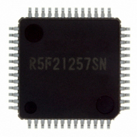
R5F21257SNFP#U0 Renesas Electronics America, R5F21257SNFP#U0 Datasheet - Page 90

R5F21257SNFP#U0
Manufacturer Part Number
R5F21257SNFP#U0
Description
IC R8C/25 MCU FLASH 52LQFP
Manufacturer
Renesas Electronics America
Series
R8C/2x/25r
Specifications of R5F21257SNFP#U0
Core Processor
R8C
Core Size
16/32-Bit
Speed
20MHz
Connectivity
I²C, LIN, SIO, SSU, UART/USART
Peripherals
POR, Voltage Detect, WDT
Number Of I /o
41
Program Memory Size
48KB (48K x 8)
Program Memory Type
FLASH
Ram Size
2.5K x 8
Voltage - Supply (vcc/vdd)
2.2 V ~ 5.5 V
Data Converters
A/D 12x10b
Oscillator Type
Internal
Operating Temperature
-20°C ~ 85°C
Package / Case
52-LQFP
For Use With
R0K521256S000BE - KIT EVAL STARTER FOR R8C/25
Lead Free Status / RoHS Status
Lead free / RoHS Compliant
Eeprom Size
-
Available stocks
Company
Part Number
Manufacturer
Quantity
Price
- Current page: 90 of 527
- Download datasheet (6Mb)
R8C/24 Group, R8C/25 Group
Rev.3.00
REJ09B0244-0300
8.
8.1
Figure 8.1
Figure 8.2
Table 8.1
Single-chip mode
Processor Mode Register 0
Processor Mode Register 1
Single-chip mode can be selected as the processor mode.
Table 8.1 lists Features of Processor Mode. Figure 8.1 shows the PM0 Register and Figure 8.2 shows the PM1
Register.
b7 b6 b5 b4
NOTE:
b7 b6 b5 b4
NOTES:
0
Processor Mode
1.
1.
2.
Processor Modes
Set the PRC1 bit in the PRCR register to 1 (w rite enable) before rew riting the PM0 register.
Set the PRC1 bit in the PRCR register to 1 (w rite enable) before rew riting the PM1 register.
The PM12 bit is set to 1 by a program (and remains unchanged even if 0 is w ritten to it).
When the CSPRO bit in the CSPR register is set to 1 (count source protect mode enabled), the PM12 bit is
automatically set to 1.
Feb 29, 2008
Processor Mode
b3 b2
b3 b2
0
PM0 Register
PM1 Register
Features of Processor Mode
b1 b0
b1 b0
0 0
0 0
Bit Symbol
Bit Symbol
(b2-b0)
(b7-b4)
(b1-b0)
(b6-b3)
Symbol
Symbol
PM03
PM12
PM0
PM1
(b7)
Page 71 of 485
—
—
—
—
—
(1)
(1)
Reserved bits
Softw are reset bit
Nothing is assigned. If necessary, set to 0.
When read, the content is 0.
Reserved bits
WDT interrupt/reset sw itch bit
Nothing is assigned. If necessary, set to 0.
When read, the content is 0.
Reserved bit
SFR, internal RAM, internal ROM All pins are I/O ports or peripheral
Address
Bit Name
0004h
Address
Bit Name
Accessible Areas
0005h
Set to 0.
The MCU is reset w hen this bit is set to 1.
When read, the content is 0.
Set to 0.
0 : Watchdog timer interrupt
1 : Watchdog timer reset
Set to 0.
function I/O pins
Pins Assignable as I/O Port Pins
After Reset
After Reset
Function
Function
00h
00h
(2)
8. Processor Mode
RW
RW
RW
RW
RW
RW
RW
—
—
Related parts for R5F21257SNFP#U0
Image
Part Number
Description
Manufacturer
Datasheet
Request
R

Part Number:
Description:
KIT STARTER FOR M16C/29
Manufacturer:
Renesas Electronics America
Datasheet:

Part Number:
Description:
KIT STARTER FOR R8C/2D
Manufacturer:
Renesas Electronics America
Datasheet:

Part Number:
Description:
R0K33062P STARTER KIT
Manufacturer:
Renesas Electronics America
Datasheet:

Part Number:
Description:
KIT STARTER FOR R8C/23 E8A
Manufacturer:
Renesas Electronics America
Datasheet:

Part Number:
Description:
KIT STARTER FOR R8C/25
Manufacturer:
Renesas Electronics America
Datasheet:

Part Number:
Description:
KIT STARTER H8S2456 SHARPE DSPLY
Manufacturer:
Renesas Electronics America
Datasheet:

Part Number:
Description:
KIT STARTER FOR R8C38C
Manufacturer:
Renesas Electronics America
Datasheet:

Part Number:
Description:
KIT STARTER FOR R8C35C
Manufacturer:
Renesas Electronics America
Datasheet:

Part Number:
Description:
KIT STARTER FOR R8CL3AC+LCD APPS
Manufacturer:
Renesas Electronics America
Datasheet:

Part Number:
Description:
KIT STARTER FOR RX610
Manufacturer:
Renesas Electronics America
Datasheet:

Part Number:
Description:
KIT STARTER FOR R32C/118
Manufacturer:
Renesas Electronics America
Datasheet:

Part Number:
Description:
KIT DEV RSK-R8C/26-29
Manufacturer:
Renesas Electronics America
Datasheet:

Part Number:
Description:
KIT STARTER FOR SH7124
Manufacturer:
Renesas Electronics America
Datasheet:

Part Number:
Description:
KIT STARTER FOR H8SX/1622
Manufacturer:
Renesas Electronics America
Datasheet:

Part Number:
Description:
KIT DEV FOR SH7203
Manufacturer:
Renesas Electronics America
Datasheet:


